If you have a related question, please click the "Ask a related question" button in the top right corner. The newly created question will be automatically linked to this question.
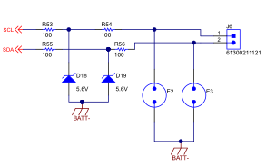
The "E" reference designators on the EVM schematic are spark gaps. These are uninsulated controlled spacing contacts which will arc at sufficient voltage to reduce ESD to the remaining circuit. Note that the EVM may show a spark gap across the FETs, this can be undesirable since it is a contamination opportunity which would bypass the protection FETs. Some designers do not like spark gaps since they are a defect opportunity and would prefer to use a component for further ESD suppression.


 这个电路是什么意思,看不懂
