This thread has been locked.

If you have a related question, please click the "Ask a related question" button in the top right corner. The newly created question will be automatically linked to this question.

DS90ub960 Routing FPD-Link III Signal Traces and PoC Filter

On dtasheet of  DS90ub960 10.1.2 (page 162)
• Consult with connector manufacturer for optimized connector footprint. If the connector is mounted on the
same side as the IC, minimize the impact of the thru-hole connector stubs by routing the high-speed signal
traces on the opposite side of the connector mounting side.
When wiring the connector,Whether the connector must be on the reverse side of the chip?

  • hello,according to the description of the datasheet, my understanding is that the connector could be the same side of the IC, but we need route the high speed signal traces on the opposite side of the connector mounting side to minimize the impact of the thru-hole connector stubs.
  • I still don't understand,Which part is referring to the thru-hole connector stubs. Does it refer to the ground via for fixing the connector? What impact will it have? Does it cause impedance discontinuity?
    On dtasheet of DS90ub960 10.2 (page 165) ,High-speed signal without layer change
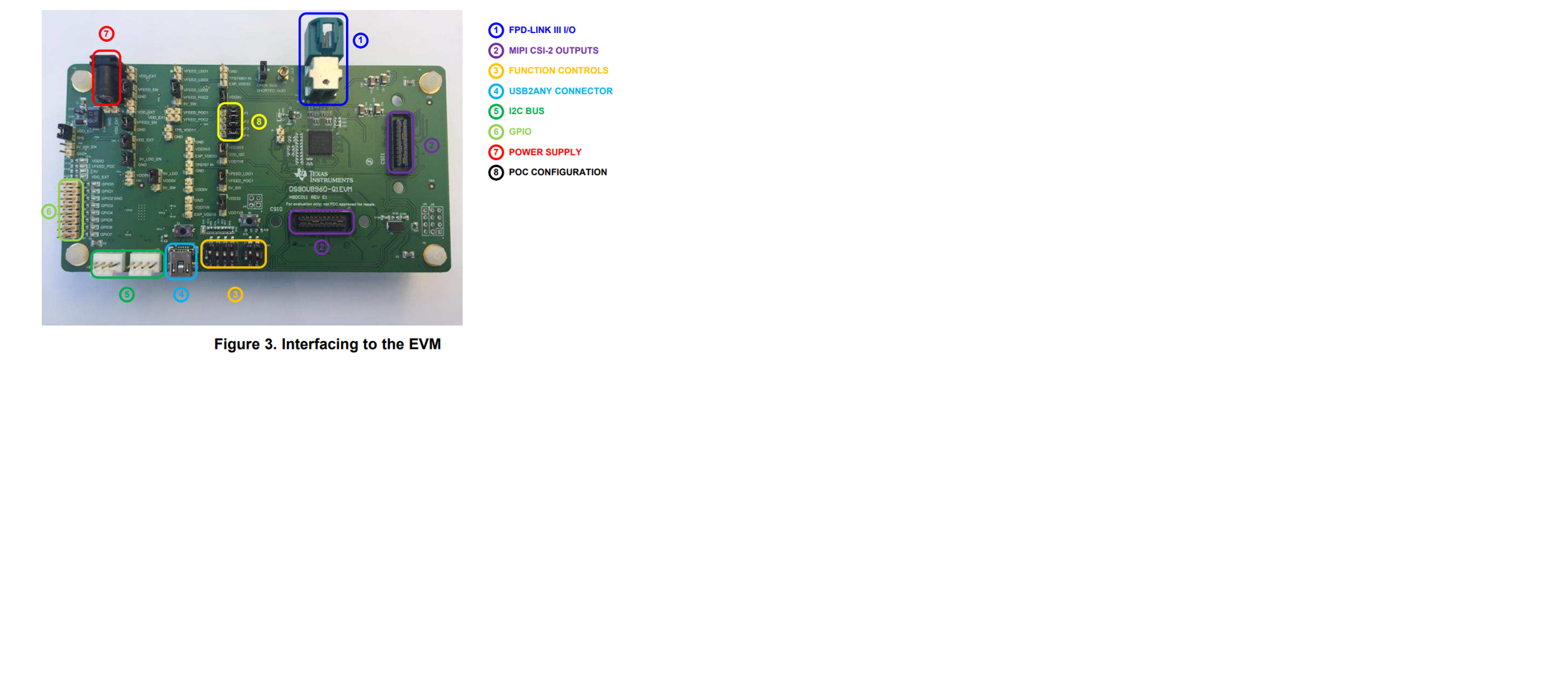
  • Hello, it means the Quad Mini-FAKRA connector. Please refer  to the  blue marked connector of the EVM user's guide:. 

    As to the impact, it mainly consider the EMI issue and the impedance discontinuity.