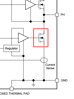
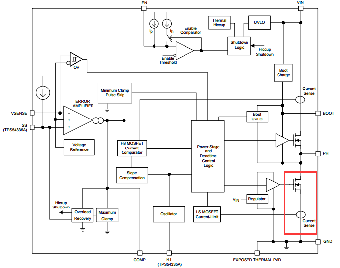
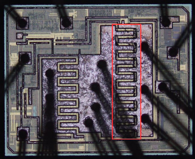
一块板子使用2片TPS54335A设计两路输出,一路输出3.3V;一路输出4V,1.2A。
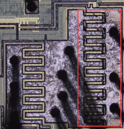
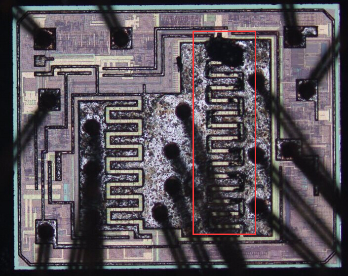
现在发现有十多片4V输出的芯片PH脚对地短路,对芯片进行FA分析,发现是由于EOS击穿。
请问根据Decap的结果,能不能判断出芯片是由于过电流还是过电压导致的击穿?
根据晶圆上的烧伤痕迹,能否看出是芯片的什么位置烧坏,是内置MOS的栅极还是电流采样被击穿?


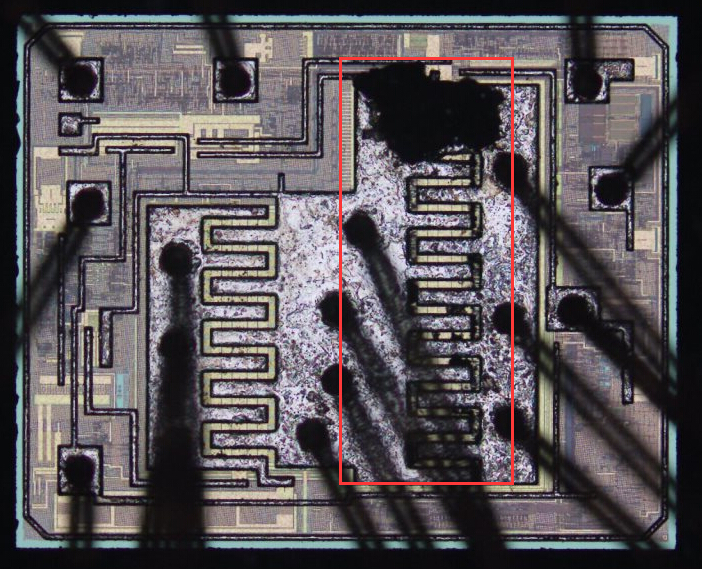
一块板子使用2片TPS54335A设计两路输出,一路输出3.3V;一路输出4V,1.2A。
现在发现有十多片4V输出的芯片PH脚对地短路,对芯片进行FA分析,发现是由于EOS击穿。
请问根据Decap的结果,能不能判断出芯片是由于过电流还是过电压导致的击穿?
根据晶圆上的烧伤痕迹,能否看出是芯片的什么位置烧坏,是内置MOS的栅极还是电流采样被击穿?