


Think of it this way. Without the ground plane the loop area is exactly defined by the placement of the components. The current must flow around the loop. If the loop is defined by a 3mm by 4mm box then the area will be 12 mm2.
When a ground plane is added, the high frequency currents on the top layer will induce an opposing current on the ground plane to cancel the magnetic field. This is often called an image current making the ground plane the image plane. This return current on the ground plane reduces the area of the loop. Think of it by laying out the loop with a piece of rope. A second rope is placed on top of the first, with the ends tied together. The loop area is now defined by twice the length of the rope multiplied by the distance between the ropes. The loop now has two layers and the area is now 28mm (twice the perimeter of the initial loop) multiplied by the distance between the two layers (0.25mm for a typical PCB stack up). The loop area is reduced to 7mm2 and a reduction in radiated energy can be achieved
此段英文为摘自SNVA638A中第6页。
按照第一段解释意思说,如果回路路径为3mm*4mm的矩形,那么其回路面积为12平方毫米(无地平面时)
按照第二段解释意思说,如果下面有地平面时,信号流在地平面会形成一个镜像路径,那么信号回流路径为下图
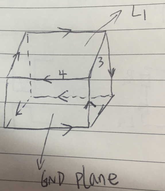
那么信号回路面积应该是(3+3+4+4)*(L1与GND PLANE的距离)
而这段解释说应该是28*(L1与GND PLANE的距离)
请问是不是我的理解有误(上图)关于“Think of it by laying out the loop with a piece of rope. A second rope is placed on top of the first, with the ends tied together. The loop area is now defined by twice the length of the rope multiplied by the distance between the ropes. The loop now has two layers and the area is now 28mm (twice the perimeter of the initial loop) multiplied by the distance between the two layers (0.25mm for a typical PCB stack up). The loop area is reduced to 7mm2 and a reduction in radiated energy can be achieved”
