This thread has been locked.

If you have a related question, please click the "Ask a related question" button in the top right corner. The newly created question will be automatically linked to this question.

我是个新手,使用CCS5.5编译出现了点问题,不知道要怎么搞

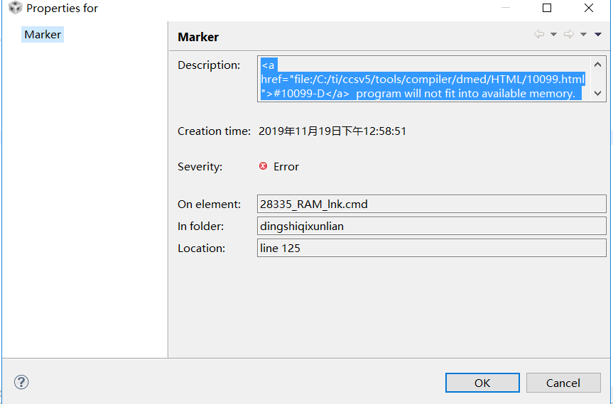
<a href="file:/C:/ti/ccsv5/tools/compiler/dmed/HTML/10099.html">#10099-D</a>  program will not fit into available memory

  • 请您详细说明下您的信息。您现在使用的板子以及程序是什么?
  • 28335,程序就是一个简单的定时器试验
    // TI File $Revision: /main/13 $
    // Checkin $Date: September 20, 2007 16:45:10 $
    //###########################################################################
    //
    // FILE: Example_2833xCpuTimer.c
    //
    // TITLE: DSP2833x Device Getting Started Program.
    //
    // ASSUMPTIONS:
    //
    // This program requires the DSP2833x header files.
    //
    // Other then boot mode configuration, no other hardware configuration
    // is required.
    //
    //
    // 根据在RAM中调试的需要,这个项目配置成"boot to SARAM".2833x引导模式
    // 表如下显示. 常用的还有"boot to Flash"模式,当程序在RAM调试完善后就
    // 可以将代码烧进Flash中并使用"boot to Flash"引导模式.
    //
    // $Boot_Table:
    //
    // GPIO87 GPIO86 GPIO85 GPIO84
    // XA15 XA14 XA13 XA12
    // PU PU PU PU
    // ==========================================
    // 1 1 1 1 Jump to Flash
    // 1 1 1 0 SCI-A boot
    // 1 1 0 1 SPI-A boot
    // 1 1 0 0 I2C-A boot
    // 1 0 1 1 eCAN-A boot
    // 1 0 1 0 McBSP-A boot
    // 1 0 0 1 Jump to XINTF x16
    // 1 0 0 0 Jump to XINTF x32
    // 0 1 1 1 Jump to OTP
    // 0 1 1 0 Parallel GPIO I/O boot
    // 0 1 0 1 Parallel XINTF boot
    // 0 1 0 0 Jump to SARAM <- "boot to SARAM"
    // 0 0 1 1 Branch to check boot mode
    // 0 0 1 0 Boot to flash, bypass ADC cal
    // 0 0 0 1 Boot to SARAM, bypass ADC cal
    // 0 0 0 0 Boot to SCI-A, bypass ADC cal
    // Boot_Table_End$
    //
    // DESCRIPTION:
    //
    // This example configures CPU Timer0, 1, and 2 and increments
    // a counter each time the timers assert an interrupt.
    //
    // Watch Variables:
    // CpuTimer0.InterruptCount
    // CpuTimer1.InterruptCount
    // CpuTimer2.InterruptCount
    //
    //###########################################################################
    // $TI Release: DSP2833x Header Files V1.01 $
    // $Release Date: September 26, 2007 $
    //###########################################################################


    #include "DSP2833x_Device.h" // DSP2833x Headerfile Include File
    #include "DSP2833x_Examples.h" // DSP2833x Examples Include File

    /***************************************************************************************************
    **Description ** 全局变量定义
    ***************************************************************************************************/
    volatile unsigned int timer_int_cnt;

    // Prototype statements for functions found within this file.
    interrupt void cpu_timer0_isr(void);
    interrupt void cpu_timer1_isr(void);
    interrupt void cpu_timer2_isr(void);
    void Gpio_select(void);


    void main(void)
    {

    // Step 1. Initialize System Control:
    // PLL, WatchDog, enable Peripheral Clocks
    // This example function is found in the DSP2833x_SysCtrl.c file.
    InitSysCtrl();

    // Step 2. Initalize GPIO:
    // This example function is found in the DSP2833x_Gpio.c file and
    // illustrates how to set the GPIO to it's default state.
    // InitGpio(); // Skipped for this example

    // 初始化使用到的GPIO口;
    Gpio_select();


    //

    DINT;

    // Initialize the PIE control registers to their default state.
    // The default state is all PIE interrupts disabled and flags
    // are cleared.
    // This function is found in the DSP2833x_PieCtrl.c file.
    InitPieCtrl();

    // Disable CPU interrupts and clear all CPU interrupt flags:
    IER = 0x0000;
    IFR = 0x0000;

    // Initialize the PIE vector table with pointers to the shell Interrupt
    // Service Routines (ISR).
    // This will populate the entire table, even if the interrupt
    // is not used in this example. This is useful for debug purposes.
    // The shell ISR routines are found in DSP2833x_DefaultIsr.c.
    // This function is found in DSP2833x_PieVect.c.
    InitPieVectTable();

    // Interrupts that are used in this example are re-mapped to
    // ISR functions found within this file.
    EALLOW; // This is needed to write to EALLOW protected registers
    PieVectTable.TINT0 = &cpu_timer0_isr;
    PieVectTable.XINT13 = &cpu_timer1_isr;
    PieVectTable.TINT2 = &cpu_timer2_isr;
    EDIS; // This is needed to disable write to EALLOW protected registers

    // Step 4. Initialize the Device Peripheral. This function can be
    // found in DSP2833x_CpuTimers.c
    InitCpuTimers(); // For this example, only initialize the Cpu Timers

    #if (CPU_FRQ_150MHZ)
    // 配置CPU定时器 0, 1, and 2 中断周期:
    // 150MHz CPU 频率, 周期单位为us;

    ConfigCpuTimer(&CpuTimer0, 150, 100000);
    ConfigCpuTimer(&CpuTimer1, 150, 200000);
    ConfigCpuTimer(&CpuTimer2, 150, 400000);
    #endif


    // To ensure precise timing, use write-only instructions to write to the entire register. Therefore, if any
    // of the configuration bits are changed in ConfigCpuTimer and InitCpuTimers (in DSP2833x_CpuTimers.h), the
    // below settings must also be updated.

    CpuTimer0Regs.TCR.all = 0x4001; // 设置TIE = 1,开启定时器0中断
    CpuTimer1Regs.TCR.all = 0x0001; // 设置TIE = 0,关闭定时器1中断
    CpuTimer2Regs.TCR.all = 0x0001; // 设置TIE = 0,关闭定时器2中断

    // Step 5. User specific code, enable interrupts:


    // Enable CPU int1 which is connected to CPU-Timer 0, CPU int13
    // which is connected to CPU-Timer 1, and CPU int 14, which is connected
    // to CPU-Timer 2:
    IER |= M_INT1;
    IER |= M_INT13;
    IER |= M_INT14;

    // Enable TINT0 in the PIE: Group 1 interrupt 7
    PieCtrlRegs.PIEIER1.bit.INTx7 = 1;

    // Enable global Interrupts and higher priority real-time debug events:
    EINT; // Enable Global interrupt INTM
    ERTM; // Enable Global realtime interrupt DBGM

    // Step 6. IDLE loop. Just sit and loop forever (optional):
    timer_int_cnt = 0;
    for(;;);

    }


    interrupt void cpu_timer0_isr(void)
    {
    CpuTimer0.InterruptCount++;

    EALLOW;
    if(timer_int_cnt++ >= 100)
    {
    timer_int_cnt = 0;
    CpuTimer0Regs.TCR.all = 0x0001; // 设置TIE = 0,关闭定时器0中断
    CpuTimer1Regs.TCR.all = 0x4001; // 设置TIE = 1,开启定时器1中断
    CpuTimer2Regs.TCR.all = 0x0001; // 设置TIE = 0,关闭定时器2中断
    }

    GpioDataRegs.GPBTOGGLE.all =0x30000000;
    GpioDataRegs.GPCTOGGLE.all =0x00000007;
    // Acknowledge this interrupt to receive more interrupts from group 1
    PieCtrlRegs.PIEACK.all = PIEACK_GROUP1;

    EDIS;
    }

    interrupt void cpu_timer1_isr(void)
    {
    CpuTimer1.InterruptCount++;

    EALLOW;

    if( timer_int_cnt++ >= 100)
    {
    timer_int_cnt = 0;
    CpuTimer0Regs.TCR.all = 0x0001; // 设置TIE = 0,关闭定时器0中断
    CpuTimer1Regs.TCR.all = 0x0001; // 设置TIE = 0,关闭定时器1中断
    CpuTimer2Regs.TCR.all = 0x4001; // 设置TIE = 1,开启定时器2中断
    }
    GpioDataRegs.GPBTOGGLE.all =0x30000000;
    GpioDataRegs.GPCTOGGLE.all =0x00000007;

    // The CPU acknowledges the interrupt.
    EDIS;
    }

    interrupt void cpu_timer2_isr(void)
    {
    CpuTimer2.InterruptCount++;
    EALLOW;
    if( timer_int_cnt++ >= 100)
    {
    timer_int_cnt = 0;
    CpuTimer0Regs.TCR.all = 0x4001; // 设置TIE = 1,开启定时器0中断
    CpuTimer1Regs.TCR.all = 0x0001; // 设置TIE = 0,关闭定时器1中断
    CpuTimer2Regs.TCR.all = 0x0001; // 设置TIE = 0,关闭定时器2中断
    }
    GpioDataRegs.GPBTOGGLE.all =0x30000000;
    GpioDataRegs.GPCTOGGLE.all =0x00000007;
    // The CPU acknowledges the interrupt.
    EDIS;
    }

    void Gpio_select(void)
    {


    EALLOW;
    GpioCtrlRegs.GPAMUX1.all = 0x00000000; // All GPIO
    GpioCtrlRegs.GPAMUX2.all = 0x00000000; // All GPIO
    GpioCtrlRegs.GPBMUX1.all = 0x00000000; // All GPIO
    GpioCtrlRegs.GPBMUX2.all = 0x00000000; // All GPIO
    GpioCtrlRegs.GPCMUX1.all = 0x00000000; // All GPIO
    GpioCtrlRegs.GPCMUX2.all = 0x00000000; // All GPIO


    GpioCtrlRegs.GPADIR.all = 0xFFFFFFFF; // All outputs
    GpioCtrlRegs.GPBDIR.all = 0xFFFFFFFF; // All outputs
    GpioCtrlRegs.GPCDIR.all = 0xFFFFFFFF; // All outputs

    GpioDataRegs.GPBDAT.all =0x30000000;
    GpioDataRegs.GPCDAT.all =0x00000007;

    EDIS;

    }

    //===========================================================================
    // No more.
    //===========================================================================
  • 我试了一下并没有出现错误(新建工程测试)

    请您右键点击错误 选择 properties 看一下具体是什么错误
  • 就是这个样子的,麻烦看一下
  • 试一下下面的link cmd文件

    /*
    // TI File $Revision: /main/11 $
    // Checkin $Date: April 15, 2009   09:57:28 $
    //###########################################################################
    //
    // FILE:    28335_RAM_lnk.cmd
    //
    // TITLE:   Linker Command File For 28335 examples that run out of RAM
    //
    //          This ONLY includes all SARAM blocks on the 28335 device.
    //          This does not include flash or OTP.
    //
    //          Keep in mind that L0 and L1 are protected by the code
    //          security module.
    //
    //          What this means is in most cases you will want to move to
    //          another memory map file which has more memory defined.
    //
    //###########################################################################
    // $TI Release:   $
    // $Release Date:   $
    //###########################################################################
    */
    
    /* ======================================================
    // For Code Composer Studio V2.2 and later
    // ---------------------------------------
    // In addition to this memory linker command file,
    // add the header linker command file directly to the project.
    // The header linker command file is required to link the
    // peripheral structures to the proper locations within
    // the memory map.
    //
    // The header linker files are found in <base>\DSP2833x_Headers\cmd
    //
    // For BIOS applications add:      DSP2833x_Headers_BIOS.cmd
    // For nonBIOS applications add:   DSP2833x_Headers_nonBIOS.cmd
    ========================================================= */
    
    /* ======================================================
    // For Code Composer Studio prior to V2.2
    // --------------------------------------
    // 1) Use one of the following -l statements to include the
    // header linker command file in the project. The header linker
    // file is required to link the peripheral structures to the proper
    // locations within the memory map                                    */
    
    /* Uncomment this line to include file only for non-BIOS applications */
    /* -l DSP2833x_Headers_nonBIOS.cmd */
    
    /* Uncomment this line to include file only for BIOS applications */
    /* -l DSP2833x_Headers_BIOS.cmd */
    
    /* 2) In your project add the path to <base>\DSP2833x_headers\cmd to the
       library search path under project->build options, linker tab,
       library search path (-i).
    /*========================================================= */
    
    /* Define the memory block start/length for the F28335
       PAGE 0 will be used to organize program sections
       PAGE 1 will be used to organize data sections
    
       Notes:
             Memory blocks on F28335 are uniform (ie same
             physical memory) in both PAGE 0 and PAGE 1.
             That is the same memory region should not be
             defined for both PAGE 0 and PAGE 1.
             Doing so will result in corruption of program
             and/or data.
    
             L0/L1/L2 and L3 memory blocks are mirrored - that is
             they can be accessed in high memory or low memory.
             For simplicity only one instance is used in this
             linker file.
    
             Contiguous SARAM memory blocks can be combined
             if required to create a larger memory block.
    */
    
    
    MEMORY
    {
    PAGE 0 :
       /* BEGIN is used for the "boot to SARAM" bootloader mode      */
    
       BEGIN      : origin = 0x000000, length = 0x000002     /* Boot to M0 will go here                      */
       RAMM0      : origin = 0x000050, length = 0x0003B0
       RAML0      : origin = 0x008000, length = 0x001000
       RAML1      : origin = 0x009000, length = 0x001000
       RAML2      : origin = 0x00A000, length = 0x001000
       RAML3      : origin = 0x00B000, length = 0x001000
       ZONE7A     : origin = 0x200000, length = 0x00FC00    /* XINTF zone 7 - program space */
       CSM_RSVD   : origin = 0x33FF80, length = 0x000076     /* Part of FLASHA.  Program with all 0x0000 when CSM is in use. */
       CSM_PWL    : origin = 0x33FFF8, length = 0x000008     /* Part of FLASHA.  CSM password locations in FLASHA            */
       ADC_CAL    : origin = 0x380080, length = 0x000009
       RESET      : origin = 0x3FFFC0, length = 0x000002
       IQTABLES   : origin = 0x3FE000, length = 0x000b50
       IQTABLES2  : origin = 0x3FEB50, length = 0x00008c
       FPUTABLES  : origin = 0x3FEBDC, length = 0x0006A0
       BOOTROM    : origin = 0x3FF27C, length = 0x000D44
    
    
    PAGE 1 :
       /* BOOT_RSVD is used by the boot ROM for stack.               */
       /* This section is only reserved to keep the BOOT ROM from    */
       /* corrupting this area during the debug process              */
    
       BOOT_RSVD  : origin = 0x000002, length = 0x00004E     /* Part of M0, BOOT rom will use this for stack */
       RAMM1      : origin = 0x000400, length = 0x000400     /* on-chip RAM block M1 */
       RAML4      : origin = 0x00C000, length = 0x001000
       RAML5      : origin = 0x00D000, length = 0x001000
       RAML6      : origin = 0x00E000, length = 0x001000
       RAML7      : origin = 0x00F000, length = 0x001000
       ZONE7B     : origin = 0x20FC00, length = 0x000400     /* XINTF zone 7 - data space */
    }
    
    
    SECTIONS
    {
       /* Setup for "boot to SARAM" mode:
          The codestart section (found in DSP28_CodeStartBranch.asm)
          re-directs execution to the start of user code.  */
       codestart        : > BEGIN,     PAGE = 0
       
    #ifdef __TI_COMPILER_VERSION__
       #if __TI_COMPILER_VERSION__ >= 15009000
        .TI.ramfunc : {} > RAML0,      PAGE = 0
       #else
       ramfuncs         : > RAML0,     PAGE = 0   
       #endif
    #endif    
       
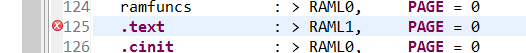
       .text            : > RAML1,     PAGE = 0
       .cinit           : > RAML0,     PAGE = 0
       .pinit           : > RAML0,     PAGE = 0
       .switch          : > RAML0,     PAGE = 0
    
       .stack           : > RAMM1,     PAGE = 1
       .ebss            : > RAML4,     PAGE = 1
       .econst          : > RAML5,     PAGE = 1
       .esysmem         : > RAMM1,     PAGE = 1
    
       IQmath           : > RAML1,     PAGE = 0
       IQmathTables     : > IQTABLES,  PAGE = 0, TYPE = NOLOAD
    
       /* Uncomment the section below if calling the IQNexp() or IQexp()
          functions from the IQMath.lib library in order to utilize the
          relevant IQ Math table in Boot ROM (This saves space and Boot ROM
          is 1 wait-state). If this section is not uncommented, IQmathTables2
          will be loaded into other memory (SARAM, Flash, etc.) and will take
          up space, but 0 wait-state is possible.
       */
       /*
       IQmathTables2    : > IQTABLES2, PAGE = 0, TYPE = NOLOAD
       {
    
                  IQmath.lib<IQNexpTable.obj> (IQmathTablesRam)
    
       }
       */
    
       FPUmathTables    : > FPUTABLES, PAGE = 0, TYPE = NOLOAD
    
       DMARAML4         : > RAML4,     PAGE = 1
       DMARAML5         : > RAML5,     PAGE = 1
       DMARAML6         : > RAML6,     PAGE = 1
       DMARAML7         : > RAML7,     PAGE = 1
    
       ZONE7DATA        : > ZONE7B,    PAGE = 1
    
       .reset           : > RESET,     PAGE = 0, TYPE = DSECT /* not used                    */
       csm_rsvd         : > CSM_RSVD   PAGE = 0, TYPE = DSECT /* not used for SARAM examples */
       csmpasswds       : > CSM_PWL    PAGE = 0, TYPE = DSECT /* not used for SARAM examples */
    
       /* Allocate ADC_cal function (pre-programmed by factory into TI reserved memory) */
       .adc_cal     : load = ADC_CAL,   PAGE = 0, TYPE = NOLOAD
    
    }
    
    /*
    //===========================================================================
    // End of file.
    //===========================================================================
    */