“线程”中讨论的其它部件: TMS320F28021, 测试
大家好,
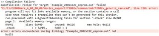
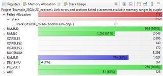
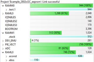
在为 将需要的几个外围设备中的两个添加代码后,TMS320F28020项目的内存很快就用完了。 该项目是一个由采用 C/C++编写的 ATmega328PB-MU 处理器提供的端口。 Atmega 部件具有32kBytes 闪存,1kByte EEPROM 和2kBytes SRAM,即使所有模块都已实现并正常工作,其内存也不会被外置。
下面是 C2000方案:
I2C 实施:
1.从“资源管理器”下载的“example_2802xI2c_eeproe.c”位字段代码开始
2.在 LaunchPadXL TMS320F2802x 上
3.在 CCS 版本中 10.4.0.00006
4.使用编译器版本 TI v21.6.0LTS
5.我添加了一个开关语句以及少量相关代码, 它有相当多的存储空间。
//########################################################################### // // FILE: Example_2802xI2c_eeprom.c // // TITLE: f2802x I2C EEPROM Example // // ASSUMPTIONS: // // This program requires the f2802x header files. // // This program requires an external I2C EEPROM connected to // the I2C bus at address 0x50. // // As supplied, this project is configured for "boot to SARAM" // operation. The 2802x Boot Mode table is shown below. // For information on configuring the boot mode of an eZdsp, // please refer to the documentation included with the eZdsp, // // $Boot_Table // While an emulator is connected to your device, the TRSTn pin = 1, // which sets the device into EMU_BOOT boot mode. In this mode, the // peripheral boot modes are as follows: // // Boot Mode: EMU_KEY EMU_BMODE // (0xD00) (0xD01) // --------------------------------------- // Wait !=0x55AA X // I/O 0x55AA 0x0000 // SCI 0x55AA 0x0001 // Wait 0x55AA 0x0002 // Get_Mode 0x55AA 0x0003 // SPI 0x55AA 0x0004 // I2C 0x55AA 0x0005 // OTP 0x55AA 0x0006 // Wait 0x55AA 0x0007 // Wait 0x55AA 0x0008 // SARAM 0x55AA 0x000A <-- "Boot to SARAM" // Flash 0x55AA 0x000B // Wait 0x55AA Other // // Write EMU_KEY to 0xD00 and EMU_BMODE to 0xD01 via the debugger // according to the Boot Mode Table above. Build/Load project, // Reset the device, and Run example // // $End_Boot_Table // // DESCRIPTION: // // This program will write 1-14 words to EEPROM and read them back. // The data written and the EEPROM address written to are contained // in the message structure, I2cMsgOut1. The data read back will be // contained in the message structure I2cMsgIn1. // // This program will work with the on-board I2C EEPROM supplied on // the F2802x eZdsp. // // //########################################################################### // $TI Release: F2802x Support Library v3.05.00.00 $ // $Release Date: 10-19-2021 $ // $Copyright: // Copyright (C) 2009-2021 Texas Instruments Incorporated - http://www.ti.com/ // // Redistribution and use in source and binary forms, with or without // modification, are permitted provided that the following conditions // are met: // // Redistributions of source code must retain the above copyright // notice, this list of conditions and the following disclaimer. // // Redistributions in binary form must reproduce the above copyright // notice, this list of conditions and the following disclaimer in the // documentation and/or other materials provided with the // distribution. // // Neither the name of Texas Instruments Incorporated nor the names of // its contributors may be used to endorse or promote products derived // from this software without specific prior written permission. // // THIS SOFTWARE IS PROVIDED BY THE COPYRIGHT HOLDERS AND CONTRIBUTORS // "AS IS" AND ANY EXPRESS OR IMPLIED WARRANTIES, INCLUDING, BUT NOT // LIMITED TO, THE IMPLIED WARRANTIES OF MERCHANTABILITY AND FITNESS FOR // A PARTICULAR PURPOSE ARE DISCLAIMED. IN NO EVENT SHALL THE COPYRIGHT // OWNER OR CONTRIBUTORS BE LIABLE FOR ANY DIRECT, INDIRECT, INCIDENTAL, // SPECIAL, EXEMPLARY, OR CONSEQUENTIAL DAMAGES (INCLUDING, BUT NOT // LIMITED TO, PROCUREMENT OF SUBSTITUTE GOODS OR SERVICES; LOSS OF USE, // DATA, OR PROFITS; OR BUSINESS INTERRUPTION) HOWEVER CAUSED AND ON ANY // THEORY OF LIABILITY, WHETHER IN CONTRACT, STRICT LIABILITY, OR TORT // (INCLUDING NEGLIGENCE OR OTHERWISE) ARISING IN ANY WAY OUT OF THE USE // OF THIS SOFTWARE, EVEN IF ADVISED OF THE POSSIBILITY OF SUCH DAMAGE. // $ //########################################################################### // // Included Files // #include "DSP28x_Project.h" // Device Headerfile and Examples Include File // // Note: I2C Macros used in this example can be found in the // f2802x_I2C_defines.h file // // // Function Prototypes // void I2CA_Init(void); uint16_t I2CA_WriteData(struct I2CMSG *msg); __interrupt void i2c_int1a_isr(void); void pass(void); void fail(void); // // Defines // #define I2C_SLAVE_ADDR 0x50 #define I2C_NUMBYTES 2 #define I2C_EEPROM_HIGH_ADDR 0x00 #define I2C_EEPROM_LOW_ADDR 0x30 // // Globals // struct I2CMSG I2cMsgOut1= { I2C_MSGSTAT_SEND_WITHSTOP, I2C_SLAVE_ADDR, I2C_NUMBYTES, I2C_EEPROM_HIGH_ADDR, I2C_EEPROM_LOW_ADDR, // // Msg Byte 1 // 0x12, // // Msg Byte 2 // 0x34 }; struct I2CMSG I2cMsgIn1= { I2C_MSGSTAT_SEND_NOSTOP, I2C_SLAVE_ADDR, I2C_NUMBYTES, I2C_EEPROM_HIGH_ADDR, I2C_EEPROM_LOW_ADDR }; uint16_t delayCounter = 0; volatile unsigned int volumeCommand[40]; volatile int redSwitchCurrent = 0; volatile int redSwitchPrevious = 0; volatile int greenSwitchCurrent = 0; volatile int greenSwitchPrevious = 0; volatile int transmitStringFlag = 0; // // Used in interrupts // struct I2CMSG *CurrentMsgPtr; uint16_t PassCount; uint16_t FailCount; volatile uint16_t idleCounter1; volatile uint16_t idleCounter2; volatile uint16_t tempByte = 0; // vv Tim's code vv //PARSING PORTION /***************************************************************************** * *****************************************************************************/ enum Command { NONE, QET, RET, SRC, QRC, QMS, IVI, DVI, SVI, QVI, SRS, QPW, SVO, IVO, DVO, QVO, SLD, SOS } ; /***************************************************************************** * *****************************************************************************/ struct CommandMessage { enum Command cmd; short value1; short value2; }; // ^^ Tim's code ^^ void TransmitString(int numBytes); struct CommandMessage cm; // This works // // Main // void main(void) { uint16_t Error; uint16_t i; // // WARNING: Always ensure you call memcpy before running any functions from // RAM InitSysCtrl includes a call to a RAM based function and without a // call to memcpy first, the processor will go "into the weeds" #ifdef _FLASH memcpy(&RamfuncsRunStart, &RamfuncsLoadStart, (size_t)&RamfuncsLoadSize); #endif // CurrentMsgPtr = &I2cMsgOut1; // // Step 1. Initialize System Control: // PLL, WatchDog, enable Peripheral Clocks // This example function is found in the f2802x_SysCtrl.c file. // InitSysCtrl(); // // Step 2. Initialize GPIO: // This example function is found in the f2802x_Gpio.c file and // illustrates how to set the GPIO to it's default state. // //InitGpio(); // // Setup only the GP I/O only for I2C functionality // InitI2CGpio(); // // Step 3. Clear all interrupts and initialize PIE vector table: // Disable CPU interrupts // DINT; // // Initialize PIE control registers to their default state. // The default state is all PIE interrupts disabled and flags // are cleared. // This function is found in the f2802x_PieCtrl.c file. // InitPieCtrl(); // // Disable CPU interrupts and clear all CPU interrupt flags // IER = 0x0000; IFR = 0x0000; // // Initialize the PIE vector table with pointers to the shell Interrupt // Service Routines (ISR). // This will populate the entire table, even if the interrupt // is not used in this example. This is useful for debug purposes. // The shell ISR routines are found in f2802x_DefaultIsr.c. // This function is found in f2802x_PieVect.c. // InitPieVectTable(); // // Interrupts that are used in this example are re-mapped to // ISR functions found within this file. // EALLOW; // This is needed to write to EALLOW protected registers PieVectTable.I2CINT1A = &i2c_int1a_isr; EDIS; // This is needed to disable write to EALLOW protected registers // // Step 4. Initialize all the Device Peripherals // I2CA_Init(); // I2C-A only // // Step 5. User specific code // // // Clear Counters // PassCount = 0; FailCount = 0; // // Clear incoming message buffer // for (i = 0; i < (I2C_MAX_BUFFER_SIZE - 2); i++) { // I2cMsgIn1.MsgBuffer[i] = 0x0000; } // // Enable interrupts required for this example // // // Enable I2C interrupt 1 in the PIE: Group 8 interrupt 1 // PieCtrlRegs.PIEIER8.bit.INTx1 = 1; // // Init GPIOs (rdv) // EALLOW; GpioCtrlRegs.GPAMUX1.bit.GPIO4 = 0; // 0 configures GPIO4 as GPIO GpioCtrlRegs.GPADIR.bit.GPIO4 = 0; // 0 makes it an input GpioCtrlRegs.GPAPUD.bit.GPIO4 = 0; // 0 enables pull-up GpioCtrlRegs.GPAMUX1.bit.GPIO5 = 0; // 0 configures GPIO5 as GPIO GpioCtrlRegs.GPADIR.bit.GPIO5 = 0; // 0 makes it an input GpioCtrlRegs.GPAPUD.bit.GPIO5 = 0; // 0 enables pull-up GpioCtrlRegs.GPAMUX2.bit.GPIO19 = 0; // 0 configures GPIO19 as GPIO GpioCtrlRegs.GPADIR.bit.GPIO19 = 1; // 1 makes it an output GpioCtrlRegs.GPAPUD.bit.GPIO19 = 0; // 0 enables pull-up EDIS; // GpioDataRegs.GPASET.bit.GPIO19 = 1; GpioDataRegs.GPACLEAR.bit.GPIO19 = 1; // // Enable CPU INT8 which is connected to PIE group 8 // IER |= M_INT8; EINT; // // Application loop // // // Temp debug vars // volumeCommand[0] = 0xfe; volumeCommand[1] = 0x51; volumeCommand[2] = 0xfe; volumeCommand[3] = 0x45; volumeCommand[4] = 0x00; volumeCommand[21] = 0xfe; volumeCommand[22] = 0x45; volumeCommand[23] = 0x40; cm.cmd = 0; cm.value1 = 0; cm.value2 = 0; for(;;) { if(delayCounter++ > 1) { delayCounter = 0; redSwitchCurrent = GpioDataRegs.GPADAT.bit.GPIO4; // Get switch states greenSwitchCurrent = GpioDataRegs.GPADAT.bit.GPIO5; if(redSwitchCurrent != redSwitchPrevious) // Compare to previous state { if(!redSwitchCurrent & redSwitchPrevious){ // If the button change is from a press, not release... transmitStringFlag = 1; cm.cmd++; if(cm.cmd > SOS) // Increment to next command { cm.cmd = NONE; // Roll to first command } } redSwitchPrevious = redSwitchCurrent; // Update previous state to current } if(greenSwitchCurrent != greenSwitchPrevious) // Compare to previous state { if(!greenSwitchCurrent & greenSwitchPrevious){ // If the button change is from a press, not release... transmitStringFlag = 1; cm.cmd--; if(cm.cmd <= NONE) // Increment to next command { cm.cmd = SOS; // Roll to first command } } greenSwitchPrevious = greenSwitchCurrent; // Update previous state to current } if(transmitStringFlag) { switch(cm.cmd) { case NONE: // 0 { short numBytes = 40; strcpy(volumeCommand+5, " NONE "); // 1234567890123456 strcpy(volumeCommand+24,"**Bottom line**. "); // 1234567890123456 volumeCommand[21] = 0xfe; TransmitString(numBytes); transmitStringFlag = 0; } break; case QET: // 1 { short numBytes = 40; strcpy(volumeCommand+5, " QET "); // 1234567890123456 strcpy(volumeCommand+24,"**Bottom line**. "); // 1234567890123456 volumeCommand[21] = 0xfe; TransmitString(numBytes); transmitStringFlag = 0; } break; case RET: // 2 { short numBytes = 40; strcpy(volumeCommand+5, " RET "); // 1234567890123456 strcpy(volumeCommand+24,"**Bottom line**. "); // 1234567890123456 volumeCommand[21] = 0xfe; TransmitString(numBytes); transmitStringFlag = 0; } break; case SRC: // 3 { short numBytes = 40; strcpy(volumeCommand+5, " SRC "); // 1234567890123456 strcpy(volumeCommand+24,"**Bottom line**. "); // 1234567890123456 volumeCommand[21] = 0xfe; TransmitString(numBytes); transmitStringFlag = 0; } break; case QRC: // 4 { short numBytes = 40; strcpy(volumeCommand+5, " QRC "); // 1234567890123456 strcpy(volumeCommand+24,"**Bottom line**. "); // 1234567890123456 volumeCommand[21] = 0xfe; TransmitString(numBytes); transmitStringFlag = 0; } break; case QMS: // 5 { short numBytes = 40; strcpy(volumeCommand+5, " QMS "); // 1234567890123456 strcpy(volumeCommand+24,"**Bottom line**. "); // 1234567890123456 volumeCommand[21] = 0xfe; TransmitString(numBytes); transmitStringFlag = 0; } break; case IVI: // 6 { short numBytes = 40; strcpy(volumeCommand+5, " IVI "); // 1234567890123456 strcpy(volumeCommand+24,"**Bottom line**. "); // 1234567890123456 volumeCommand[21] = 0xfe; TransmitString(numBytes); transmitStringFlag = 0; } break; case DVI: // 7 { short numBytes = 40; strcpy(volumeCommand+5, " DVI "); // 1234567890123456 strcpy(volumeCommand+24,"**Bottom line**. "); // 1234567890123456 volumeCommand[21] = 0xfe; TransmitString(numBytes); transmitStringFlag = 0; } break; case SVI: // 8 { short numBytes = 40; strcpy(volumeCommand+5, " SVI "); // 1234567890123456 strcpy(volumeCommand+24,"**Bottom line**. "); // 1234567890123456 volumeCommand[21] = 0xfe; TransmitString(numBytes); transmitStringFlag = 0; } break; case QVI: // 9 { short numBytes = 40; strcpy(volumeCommand+5, " QVI "); // 1234567890123456 strcpy(volumeCommand+24,"**Bottom line**. "); // 1234567890123456 volumeCommand[21] = 0xfe; TransmitString(numBytes); transmitStringFlag = 0; } break; case SRS: // 10 { short numBytes = 40; strcpy(volumeCommand+5, " SRS "); // 1234567890123456 strcpy(volumeCommand+24,"**Bottom line**. "); // 1234567890123456 volumeCommand[21] = 0xfe; TransmitString(numBytes); transmitStringFlag = 0; } break; case QPW: // 11 { short numBytes = 40; strcpy(volumeCommand+5, " QPW "); // 1234567890123456 strcpy(volumeCommand+24,"**Bottom line**. "); // 1234567890123456 volumeCommand[21] = 0xfe; TransmitString(numBytes); transmitStringFlag = 0; } break; case SVO: // 12 { short numBytes = 40; strcpy(volumeCommand+5, " SVO "); // 1234567890123456 strcpy(volumeCommand+24,"**Bottom line**. "); // 1234567890123456 volumeCommand[21] = 0xfe; TransmitString(numBytes); transmitStringFlag = 0; } break; case IVO: // 13 { short numBytes = 40; strcpy(volumeCommand+5, " IVO "); // 1234567890123456 strcpy(volumeCommand+24,"**Bottom line**. "); // 1234567890123456 volumeCommand[21] = 0xfe; TransmitString(numBytes); transmitStringFlag = 0; } break; case DVO: // 14 { short numBytes = 40; strcpy(volumeCommand+5, " DVO "); // 1234567890123456 strcpy(volumeCommand+24,"**Bottom line**. "); // 1234567890123456 volumeCommand[21] = 0xfe; TransmitString(numBytes); transmitStringFlag = 0; } break; case QVO: // 15 { short numBytes = 40; strcpy(volumeCommand+5, " QVO "); // 1234567890123456 strcpy(volumeCommand+24,"**Bottom line**. "); // 1234567890123456 volumeCommand[21] = 0xfe; TransmitString(numBytes); transmitStringFlag = 0; } break; case SLD: // 16 { short numBytes = 40; strcpy(volumeCommand+5, " SLD "); // 1234567890123456 strcpy(volumeCommand+24,"**Bottom line**. "); // 1234567890123456 volumeCommand[21] = 0xfe; TransmitString(numBytes); transmitStringFlag = 0; } break; case SOS: // 17 { short numBytes = 40; strcpy(volumeCommand+5, " SOS "); // 1234567890123456 strcpy(volumeCommand+24,"**Bottom line**. "); // 1234567890123456 volumeCommand[21] = 0xfe; TransmitString(numBytes); transmitStringFlag = 0; } break; default: // Anything else { short numBytes = 40; strcpy(volumeCommand+5, " Command "); // 1234567890123456 strcpy(volumeCommand+24,"was out of range"); // 1234567890123456 volumeCommand[21] = 0xfe; TransmitString(numBytes); transmitStringFlag = 0; } break; } } } } } // // I2CA_Init - // void I2CA_Init(void) { // Initialize I2C I2caRegs.I2CMDR.bit.IRS = 0; // SEE BELOW - Put I2C module in reset while making changes // // Own Address Register // // Bit 15: READ ONLY - Reserved I2caRegs.I2COAR = 0x26; // Own address = 0x28 // Bits 7-15: Reserved // // I2C Interrupt Enable Register // // Bits 7-15: READ ONLY - Reserved I2caRegs.I2CIER.bit.AAS = 0; // Bit 6: 1 = Addressed as slave interrupt request enabled I2caRegs.I2CIER.bit.SCD = 0; // Bit 5: 1 = Stop condition detected interrupt request enabled I2caRegs.I2CIER.bit.XRDY = 0; // Bit 4: 1 = Transmit data ready interrupt request disabled I2caRegs.I2CIER.bit.RRDY = 0; // Bit 3: 1 = W1C - Receive data ready interrupt request enabled I2caRegs.I2CIER.bit.ARDY = 0; // Bit 2: 1 = Master Only - Register access ready interrupt request enabled I2caRegs.I2CIER.bit.NACK = 0; // Bit 1: 0 = W1C - No-ack interrupt request disabled I2caRegs.I2CIER.bit.ARBL = 0; // Bit 0: 0 = W1C - Arbitration lost interrupt request disabled // // I2C Status Register // // Bit 15: READ ONLY - Reserved I2caRegs.I2CSTR.bit.SDIR = 1; // Bit 14: W1C - Slave direction bit 0 = not addressed as slave transmitter I2caRegs.I2CSTR.bit.NACKSNT = 1; // Bit 13: W1C - NACK sent bit 0 = NACK not sent I2caRegs.I2CSTR.bit.BB = 0; // Bit 12: Bus Busy bit 0 = bus free I2caRegs.I2CSTR.bit.RSFULL = 0; // Bit 11: 1 = receive shift register overrun condition detected I2caRegs.I2CSTR.bit.XSMT = 0; // Bit 10: 0 = transmit shift register underflow detected (empty) I2caRegs.I2CSTR.bit.AAS = 0; // Bit 9: 1 = I2C module recognized its own slave address I2caRegs.I2CSTR.bit.AD0 = 0; // Bit 8: 1 = address of all zeros (general call) was detected // Bits 6-7: READ ONLY - Reserved I2caRegs.I2CSTR.bit.SCD = 1; // Bit 5: W1C - 1 = stop condition was detected I2caRegs.I2CSTR.bit.XRDY = 1; // Bit 4: 1 = Ready for more transmit data to go in I2CDXR I2caRegs.I2CSTR.bit.RRDY = 1; // Bit 3: W1C - Receive data ready int flag 1 = data is in I2CDRR I2caRegs.I2CSTR.bit.ARDY = 1; // Bit 2: Master Only - Register access ready int flag I2caRegs.I2CSTR.bit.NACK = 1; // Bit 1: W1C - 1 = NACK received I2caRegs.I2CSTR.bit.ARBL = 1; // Bit 0: W1C - 1 = arbitration lost // // I2C Clock Prescale Register // // Setup I2C data rate I2caRegs.I2CPSC.bit.IPSC = 5; // Prescaler value 60mHz SYSCLK / 6 = 10mHz (5+1=6) // // I2C Clock high-time and low-time Registers // // 10mHz / 200 = 50kHz for comm's with 2x16 debugging display I2caRegs.I2CCLKL = 129; // 129 + 5 = 136 I2caRegs.I2CCLKH = 61; // 61 + 5 = 66 // // Data Count Register // I2caRegs.I2CCNT = 1; // Bits 0-15: Set data count (ignored in RM mode) // Is changed to actual number of bytes to transfer when in // transmit mode. // // Slave Address Register // // Bits 10-15: READ ONLY - Reserved I2caRegs.I2CSAR = 0x28; // Bits 0-9: Address to which data will be transmitted (Master only) // // I2C Mode Register // // Bits 14-15: READ ONLY - Reserved I2caRegs.I2CMDR.bit.NACKMOD = 0; // Bit 15: NACK mode I2caRegs.I2CMDR.bit.FREE = 0; // Bit 14: For debugging: 0 = I2C halts during interrupts // I2caRegs.I2CMDR.bit.STT = 0; // Bit 13: Master only - Start bit Can't be written when IRS=0 // Bit 12: Reserved // I2caRegs.I2CMDR.bit.STP = 0; // Bit 11: Master only - Stop bit Can't be written when IRS=0 I2caRegs.I2CMDR.bit.MST = 1; // Bit 10: Remains 0 for slave mode. 1 = Master mode I2caRegs.I2CMDR.bit.TRX = 1; // Bit 9: 0 = Receive mode, 1 = Transmit mode I2caRegs.I2CMDR.bit.XA = 0; // Bit 8: 0 = 7 bit address mode I2caRegs.I2CMDR.bit.RM = 1; // Bit 7: 1 = repeat mode I2caRegs.I2CMDR.bit.DLB = 0; // Bit 6: 0 = Digital loopback mode disabled // I2caRegs.I2CMDR.bit.IRS = 1; // Bit 5: I2C module is re-enabled after making changes I2caRegs.I2CMDR.bit.STB = 0; // Bit 4: Master only - Start Byte mode I2caRegs.I2CMDR.bit.FDF = 0; // Bit 3: Keep at 0. Free data format mode I2caRegs.I2CMDR.bit.BC = 0; // Bits 0-2: Set bit count to 8 bits (0 = 8) // // I2C Extended Mode Register // // Bits 1-15: READ ONLY - Reserved I2caRegs.I2CEMDR.bit.BCM = 0; // Bit 0: Backwards compatibility mode // // Transmit FIFO Register // // Bits 14-15: READ ONLY - Reserved // Bit 15: Reserved I2caRegs.I2CFFTX.bit.I2CFFEN = 0; // Bit 14: 1 = Enable transmit & receive FIFOs I2caRegs.I2CFFTX.bit.TXFFRST = 0; // Bit 13: 1 = Take transmit FIFO out of reset // I2caRegs.I2CFFTX.bit.TXFFST = 0; // Bits 8-12: READ ONLY - How many bytes are in the transmit FIFO // I2caRegs.I2CFFTX.bit.TXFFINT = 0; // Bit 7: READ ONLY - 1 = interrupt occurred I2caRegs.I2CFFTX.bit.TXFFINTCLR = 1; // Bit 6: W1C - Clears transmit interrupt flag (do again after irs = 1) I2caRegs.I2CFFTX.bit.TXFFIENA = 0; // Bit 5: 0 = Disable transmit FIFO interrupt I2caRegs.I2CFFTX.bit.TXFFIL = 0; // Bits 0-4: Set the transmit FIFO interrupt Threshold // // Receive FIFO Register // // Bits 14-15: READ ONLY - Reserved I2caRegs.I2CFFRX.bit.RXFFRST = 0; // Bit 13: 1 = enable receive FIFO operation // I2caRegs.I2CFFRX.bit.RXFFST = 0; // BitS 8-12: READ ONLY - Bytes in receive FIFO // I2caRegs.I2CFFRX.bit.RXFFINT = 0; // Bit 7: READ ONLY - Receive interrupt flag 1 = int I2caRegs.I2CFFRX.bit.RXFFINTCLR = 1; // Bit 6: Write 1 to clear receive int flag I2caRegs.I2CFFRX.bit.RXFFIENA = 0; // Bit 5: 1 = receive interrupt is enabled I2caRegs.I2CFFRX.bit.RXFFIL = 0; // Bits 0-4: Set the receive FIFO interrupt level // Clean up and exit I2caRegs.I2CMDR.bit.IRS = 1; // SEE ABOVE - I2C module is re-enabled after making changes I2caRegs.I2CFFTX.bit.TXFFINTCLR = 1; // SEE ABOVE - Clears transmit interrupt flag I2caRegs.I2CFFRX.bit.RXFFINTCLR = 1; // SEE ABOVE - Clears receive interrupt flag return; } // // Transmit String - // void TransmitString(int numBytes) { uint16_t i; uint16_t i2; // wait for STOP condition while (I2caRegs.I2CMDR.bit.STP != 0); //bus is not occupied // generate START condition I2caRegs.I2CMDR.bit.STT = 1;// resets once the START condition is issued for(i = 0; i < numBytes; i++){ idleCounter1 = 0; while(!I2caRegs.I2CSTR.bit.XRDY) { if(idleCounter1++ >= 60000) // 30,000 ~ 12.6ms // When the master read happens before data is ready (after the master sends a write) // XRDY is never satisfied. This algorithm senses this condition and after a time // (~12.6ms) reads the I2CDRR to clear the I2C bus condition. // Extending this delay makes the data transfer more robust, but at the expense of // extending the GMS trip response (during this delay). // // // This is to help unstick the bus when too many writes are issued { // by master w/o reading. It must be long enough to allow master idleCounter1 = 0; // enough time to download bytes normally. tempByte = I2caRegs.I2CDRR; // It must be short enough to allow quick end to CPU hogging // The following resets I2C xmit buffer in case master doesn't pull all data I2caRegs.I2CMDR.bit.IRS = 0; // Put I2C module in reset while making changes I2caRegs.I2CCNT = 0; // Set data count to 0 clears xmit buffer I2caRegs.I2CMDR.bit.IRS = 1; // I2C module is re-enabled after making changes } } // wait for XRDY flag to transmit data // while (I2caRegs.I2CSTR.bit.XRDY != 1);//wait for the XRDY (transmit mode ready) bit of the status register, which means that the data transmit register is ready to accept new data. I2caRegs.I2CDXR = volumeCommand[i]; // Loads a value into the data xmit buffer, starting the xmit process // I2caRegs.I2CMDR.all = 0x6E20; for(i2=0; i2<2500; i2++) { // Do nothing, just wait } } // snd stop condition here I2caRegs.I2CMDR.bit.STP = 1; /* idleCounter2 = 0; while(I2caRegs.I2CSTR.bit.BB) { if(idleCounter2++ >= 1000) // This is to help unstick the bus when xmit buffer empties { idleCounter2 = 0; I2caRegs.I2CDXR = 0xdb; } } */ I2caRegs.I2CMDR.all = 0x06a0; // Resets the I2C mode register } uint16_t I2CA_WriteData(struct I2CMSG *msg) { uint16_t i; uint16_t i2; // wait for STOP condition while (I2caRegs.I2CMDR.bit.STP != 0); //bus is not occupied // generate START condition I2caRegs.I2CMDR.bit.STT = 1;// resets once the START condition is issued for(i = 0; i < 40; i++){ idleCounter1 = 0; while(!I2caRegs.I2CSTR.bit.XRDY) { if(idleCounter1++ >= 60000) // 30,000 ~ 12.6ms // When the master read happens before data is ready (after the master sends a write) // XRDY is never satisfied. This algorithm senses this condition and after a time // (~12.6ms) reads the I2CDRR to clear the I2C bus condition. // Extending this delay makes the data transfer more robust, but at the expense of // extending the GMS trip response (during this delay). // // // This is to help unstick the bus when too many writes are issued { // by master w/o reading. It must be long enough to allow master idleCounter1 = 0; // enough time to download bytes normally. tempByte = I2caRegs.I2CDRR; // It must be short enough to allow quick end to CPU hogging // The following resets I2C xmit buffer in case master doesn't pull all data I2caRegs.I2CMDR.bit.IRS = 0; // Put I2C module in reset while making changes I2caRegs.I2CCNT = 0; // Set data count to 0 clears xmit buffer I2caRegs.I2CMDR.bit.IRS = 1; // I2C module is re-enabled after making changes } } // wait for XRDY flag to transmit data // while (I2caRegs.I2CSTR.bit.XRDY != 1);//wait for the XRDY (transmit mode ready) bit of the status register, which means that the data transmit register is ready to accept new data. // generate START condition // I2caRegs.I2CMDR.bit.STT = 1;// resets once the START condition is issued I2caRegs.I2CDXR = volumeCommand[i]; // Loads a value into the data xmit buffer, starting the xmit process // I2caRegs.I2CMDR.all = 0x6E20; for(i2=0; i2<2500; i2++) { // Do nothing, just wait } } // snd stop condition here I2caRegs.I2CMDR.bit.STP = 1; idleCounter2 = 0; while(I2caRegs.I2CSTR.bit.BB) { if(idleCounter2++ >= 1000) // This is to help unstick the bus when xmit buffer empties { idleCounter2 = 0; I2caRegs.I2CDXR = 0xdb; } } I2caRegs.I2CMDR.all = 0x06a0; // Resets the I2C mode register return I2C_SUCCESS; } // // i2c_int1a_isr - I2C-A // __interrupt void i2c_int1a_isr(void) { uint16_t IntSource, i; // // Read interrupt source // IntSource = I2caRegs.I2CISRC.all; // // Interrupt source = stop condition detected // if(IntSource == I2C_SCD_ISRC) { // // If completed message was writing data, reset msg to inactive state // if (CurrentMsgPtr->MsgStatus == I2C_MSGSTAT_WRITE_BUSY) { CurrentMsgPtr->MsgStatus = I2C_MSGSTAT_INACTIVE; } else { // // If a message receives a NACK during the address setup portion // of the EEPROM read, the code further below included in the // register access ready interrupt source code will generate a stop // condition. After the stop condition is received (here), set the // message status to try again. User may want to limit the number // of retries before generating an error. // if(CurrentMsgPtr->MsgStatus == I2C_MSGSTAT_SEND_NOSTOP_BUSY) { CurrentMsgPtr->MsgStatus = I2C_MSGSTAT_SEND_NOSTOP; } // // If completed message was reading EEPROM data, reset msg to // inactive state and read data from FIFO. // else if (CurrentMsgPtr->MsgStatus == I2C_MSGSTAT_READ_BUSY) { CurrentMsgPtr->MsgStatus = I2C_MSGSTAT_INACTIVE; for(i=0; i < I2C_NUMBYTES; i++) { CurrentMsgPtr->MsgBuffer[i] = I2caRegs.I2CDRR; } // // Check received data // for(i=0; i < I2C_NUMBYTES; i++) { if(I2cMsgIn1.MsgBuffer[i] == I2cMsgOut1.MsgBuffer[i]) { PassCount++; } else { FailCount++; } } if(PassCount == I2C_NUMBYTES) { pass(); } else { fail(); } } } } // // Interrupt source = Register Access Ready // This interrupt is used to determine when the EEPROM address setup // portion of the read data communication is complete. Since no stop bit is // commanded, this flag tells us when the message has been sent instead of // the SCD flag. If a NACK is received, clear the NACK bit and command a // stop. Otherwise, move on to the read data portion of the communication. // else if(IntSource == I2C_ARDY_ISRC) { if(I2caRegs.I2CSTR.bit.NACK == 1) { I2caRegs.I2CMDR.bit.STP = 1; I2caRegs.I2CSTR.all = I2C_CLR_NACK_BIT; } else if(CurrentMsgPtr->MsgStatus == I2C_MSGSTAT_SEND_NOSTOP_BUSY) { CurrentMsgPtr->MsgStatus = I2C_MSGSTAT_RESTART; } } else { // // Generate some error due to invalid interrupt source // __asm(" ESTOP0"); } // // Enable future I2C (PIE Group 8) interrupts // PieCtrlRegs.PIEACK.all = PIEACK_GROUP8; } // // pass - // void pass() { __asm(" ESTOP0"); for(;;); } // // fail - // void fail() { __asm(" ESTOP0"); for(;;); } // // End of File //
SCIA 实施:
1.运行从“资源管理器”下载的“example_2802xScia_FFDLB.c”位字段代码
2.在 LaunchPadXL TMS320F2802x 上
3.在 CCS 版本中 10.4.0.00006
4.使用编译器版本 TI v21.6.0LTS
由于内存不足,我无法让这两个模块一起运行。 我仍需要为以下项目添加功能:
1,ADC
2.GPIO
3.闪存 IO
4.用户界面
问题:
1. Atmega 部件是8位处理器,而28020是32位处理器。 假设8位部分的32 KB 内存中的哪些内容可以在32位部分中容纳32 KB,这是不对的?
2.在保持简单 I2C 和 SCIA 通信的能力的同时,可以消除大量的示例代码吗? 对于 I2C,28020是主数据,从数据不会响应(仅 ACK)。
3.对于64k,我可以切换到 TMS320F28021,但这是否足够?
如果有人能提供帮助,我将不胜感激。
谢谢,
罗宾