


有关SA如何与ADC输入互连的文档似乎不完整或至少令人困惑!
请参阅6.10 17交叉芯片互联(msp430fr2355.pdf的第83页),
我们看到SAC0 OA输出(OA0O)在绘图左侧显示一个带有X的正方形。
该处被标记为1.1 ,OA0O,0.1 ,A1
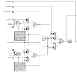
6.11 1端口P1输入/输出(同一文档的第95页)在左上角显示一行(到或从?) ... A1,... OA...,COMP0...和端口P1引脚。
以下第96页建议将“OA0O,0.1 ,A1”的P1SELx设置为11。
在同一页上,它指出,如果要将WFP的1.1 用于I/O,则P1SELx应设置为0 (大概是此处为00?),同时设置P1DIR以定义输入还是输出。
文件没有表明可以同时将输出内部路由到A1,同时使用WFP 1.1 进行I/O操作!
同样,它也没有指明如果确实可能的话,P1SELx和P1DIR的适当设置是什么(因为我的实验似乎表明是这样)。
我的目标是使用SAC0 (例如,在相关引脚上有一个输入信号,即WFP 1.2 和WFP 1.3),将输出路由到内部A1,以测量信号。
同时,我想将WFP插脚1.1 用于其他目的,即I/O
(这样就可以获得一个'免费'的额外引脚! 我的设计缺少针脚...)
(SAC1的输出可以在内部路由到A5,这同样适用于SAC1。)
我已使用以下代码或多或少地回答了我自己的问题。
对于"OA0O,0.1 ,A1",我将P1SELx设置为11。
我不使用P1DIR做任何事情-因此它的默认值为0,即引脚1.1 在理论上是输入。
尽管如此,我还是能够驱动代码中的针脚H和L来使LED闪烁!
因此,虽然我可能已经用“是的,这似乎是可能的”回答了我的问题,但我有一些担心,我可能会以某种方式滥用MSP430?
可能是使用了WFP 1.1 作为输出(尽管P1DIR为0!) 是否会对其驱动器功能产生影响?
或者是否会对A1产生影响(换用WFP 1.1 时产生的噪音峰值等)?
我还测试了P1DIR,如我的评论所述:
;无论是否使用以下行,功能都是相同的!!!
;BIS.b #BIT1,&P1DIR; WFP 1.1 作为输出(用于驱动外部LED)
我还没有测试过是否可以将WFP 1.1 用作输入。
(假设如果可以,P1DIR将保持其默认设置0?)
[是否与P1OUT和P1IN发生冲突?!!]
总之,请检查我所做的事情是否正常,而不会导致任何潜在的问题...
(对驱动器功能的影响,P1OUT和P1IN之间的冲突,对ADC转换性能的影响...?)
此外,请考虑改进相关文档。
这是我的代码,用于尝试调查正在发生的情况:
SAC0生成一个斜坡信号,该信号在内部路由到A1。
启动板上的绿色和红色LED指示信号测量值分别低于或高于2V。
在主环路中,我会闪存一个由WFP 1.1 驱动的外部LED指示灯,以证明当SAC0驱动ADC的A1时,该引脚可用于输出。
;-------------------------------------------------------------------------------
;
;  Attempt to use P1.1 for I/O at same time as SAC OA0O drives A1 ADC
;  Starting point was: (my project Asm_SAC_L3_05)
;  MSP430FR235x Demo - SAC-L3, DAC Buffer Mode
;
;  Description: Configure SAC-L3 for DAC Buffer Mode.
;  Use the 12 bit DAC to output positive ramp.
;  The OA is set in buffer mode to improve DAC output drive strength.
;  Internal 2.5V reference is selected as DAC reference.
;  Observe the output of OA0O pin with oscilloscope.
;  ACLK = n/a, MCLK = SMCLK = default DCODIV ~1MHz.
;
;  Note: period of ramp measures as 504.5 msec (need to check SMCLK freq. and study the timer theory!)
;
;                MSP430FR235x
;             -------------------
;         /|\|                   |
;          | |                   |
;          --|RST     DAC12->OA0O|--> oscilloscope
;            |                   |
;            |                   |
;            |                   |
;            |                   |
;            |                   |
;
;   Darren Lu, TI
;   + own additions ...
;
;-------------------------------------------------------------------------------
            .cdecls C,LIST,"msp430.h"       ; Include device header file

;-------------------------------------------------------------------------------
            .def    RESET                   ; Export program entry-point to
                                            ; make it known to linker.
;-------------------------------------------------------------------------------
            .text                           ; Assemble into program memory.
            .retain                         ; Override ELF conditional linking
                                            ; and retain current section.
            .retainrefs                     ; And retain any sections that have
                                            ; references to current section.

            .global	ADC_Value				; This is necessary to have ADC_Value recognised in the Expressions window!
			.data
			.bss ADC_Value, 2
			.text

;-------------------------------------------------------------------------------
RESET       mov.w   #__STACK_END,SP         ; Initialiwe stackpointer
StopWDT     mov.w   #WDTPW|WDTHOLD,&WDTCTL  ; Stop watchdog timer

            ; Disable the GPIO power-on default high-impedance mode
            ; to activate previously configured port settings
            bic.w   #LOCKLPM5,&PM5CTL0      ; (Turn off digital I/O)

            mov.b   #PMMPW_H,&PMMCTL0_H     ; Unlock the PMM registers
            mov.w   #INTREFEN+REFVSEL_2,&PMMCTL2; Enable internal 2.5V reference
PollRef     bit.w   #REFGENRDY,&PMMCTL2     ; Poll till internal reference settles
            jz      PollRef                 ;

; Despite the following settings for P1SEL0 and P1SEL1, I am still also able to use P1.1 as an independent output!
SetPin      bis.b   #BIT1,&P1SEL0           ; Select P1.1 as OA0O function
            bis.b   #BIT1,&P1SEL1           ; OA is used as buffer for DAC.

            mov.w   #DACSREF_1+DACLSEL_2+DACIE,&SAC0DAC; Select (2.5V, defined above) int Vref as DAC ref,
            								; DAC always loads data from DACDAT at the +ve edge of TB2.1B signal,
            								; Enable DAC interrupt
            ;mov.w   #0,R13
            ;clr.w   R13
            ;mov.w   R13,&SAC0DAT            ; Initial DAC data
            clr.w   &SAC0DAT                ; Initial DAC data=0 (DHBR simplification not involving use of R13)
            bis.w   #DACEN,&SAC0DAC         ; Enable DAC

            mov.w   #NMUXEN+PMUXEN+PSEL_1+NSEL_1,&SAC0OA; Enable negative (follower) and positive (DAC) input
            bis.w   #OAPM,&SAC0OA           ; Select low speed and low power mode
            mov.w   #MSEL_1,&SAC0PGA        ; Set OA as buffer mode
            bis.w   #SACEN+OAEN,&SAC0OA     ; Enable SAC and OA

            ; Use TB2.1B as DAC hardware trigger
            mov.w   #0x63,&TB2CCR0          ; PWM Period/2
            mov.w   #OUTMOD_6,&TB2CCTL1;    ; TBCCR1 toggle/set
            mov.w   #0x32,&TB2CCR1          ; TBCCR1 PWM duty cycle
            mov.w   #TBSSEL__SMCLK+MC_1+TBCLR,&TB2CTL ; SMCLK, up mode, clear TB2R

; -- Configure ports for LEDs (based on code from Asm_ADC_Sampling_P1.2_LPM)
			;bic.b	#BIT0, &P1OUT           ; LED1 (red) = 0 (Off)
			bis.b	#BIT0, &P1DIR			; Configure LED1 (red) as output
			;bic.b	#BIT6, &P6OUT           ; LED2 (green) = 0 (Off)
			bis.b	#BIT6, &P6DIR			; Configure LED2 (green) as output

			; Functionality is the same whether or not following line is used!!!
			;bis.b	#BIT1, &P1DIR			; P1.1 as output (to drive external LED)

 			bic.b	#LOCKLPM5, &PM5CTL0		; Turn on digital I/O

; -- setup ADC (based on code from Asm_ADC_Sampling_P1.2_LPM)
           	bic.w	#ADCSHT0, &ADCCTL0		; Clear bit 0 (bit 8 of register) of default ADCSHT=01
			bis.w	#ADCSHT1, &ADCCTL0		; Conversion = 16 ADCCLK cycles (0010b)
			;mov.w   #ADCSHT_2|ADCON, &ADCCTL0 ; Conversion = 16 ADCCLK cycles (0010b).  Hao uses instead of the above two lines.
			bis.w	#ADCON, &ADCCTL0		; Turn ADC on

			bis.w	#ADCSSEL_3, &ADCCTL1	; ADC clock signal = SMCLK (1MHz).  Hao uses the default MODOSC (MODCLK).  msp430fr2355 page 68: 3.8MHz +/- 21%
			bis.w	#ADCSHP_1, &ADCCTL1		; SAMPCON signal is sourced from the sampling timer

			bic.w	#ADCRES0, &ADCCTL2		;
			bis.w	#ADCRES_2, &ADCCTL2		; Resolution = 12-bit (ADRED=10)

			bis.w	#ADCINCH_1, &ADCMCTL0	; ADC input channel A1 (P1.1) (hoping to be able to use P1.1 also for I/O?!)

			bis.w	#ADCIE0, &ADCIE			; Enable ADC conversion complete IRQ

			bis.w	#ADCENC|ADCSC, &ADCCTL0 ; Enable and start ADC conversion

            ;nop
            ;bis.w   #LPM3+GIE,SR            ; Enter LPM3, Enable Interrupt  For Lu (and here) code will sit here, with interrupts continuing to be serviced.
            ;nop

            nop
            bis.w   #GIE,SR            		; Enable global interrupts
            nop

main:
			bis.w   #LPM3,SR            	; Enter LPM3

			bis.w	#ADCENC|ADCSC, &ADCCTL0 ; Enable and start ADC conversion

			clr.w	R4
DelayLoop   inc.w	R4				; Based on Davies page 95 (approx 0.7 sec)
			cmp.w   #50000,R4
			jne		DelayLoop
            xor.b	#BIT1, &P1OUT   ; toggle LED


			jmp		main

;-------------------------------------------------------------------------------
; ISR for SAC0 (note that shares same vector as for SAC2)
;-------------------------------------------------------------------------------
SAC0_ISR:   add.w   &SAC0IV,PC
            reti                            ; Vector  0: No interrupt
            reti                            ; Vector  2: (reserved)
            ;jmp     SACDACMODE              ; Vector  4: SAC DAC Interrupt (other vectors are reserved)
;SACDACMODE
			;add.w  #1,R13                   ;
            ;and.w  #0xFFF,R13               ;
            ;mov.w  R13,&SAC0DAT             ; DAC12 output positive ramp
            inc.w  &SAC0DAT					; DAC12 output positive ramp (DHBR simplification not involving use of R13)
            bic.w	#LPM3, 0(SP)			; Cancel LPM3 on exit. i.e., return to active mode
            reti


; Code would be more robust if check ADCIV register.
; There could be other interrupts for overflows, etc.
; Hao code does this.  Note that, with his code, other types of interrupt will not result in exit from LPM0.  That is okay/ correct!
ADC_ISR:
            ;mov.w   &ADCIV, PC				; Add offset to PC and clear the associated interrupt
            ; ...
			mov.w   &ADCMEM0, ADC_Value     ; No need for own variable!  Could use &ADCMEM0 in following (but would flag be cleared?)!  Or R4.
			;mov.w   &ADCMEM0, R4
			cmp.w   #2482, ADC_Value
			;cmp.w   #1000, ADC_Value
			;cmp.w   #1000, R4
			jhs     ge2V
		    bic.b	#BIT0, &P1OUT			; For A2 < 2V: LED1 (red) OFF
		    bis.b	#BIT6, &P6OUT			; 			   LED2 (green) ON
			jmp		ADC_ISR_end
ge2V:		bis.b	#BIT0, &P1OUT			; For A2 >= 2V: LED1 (red) ON
		    bic.b	#BIT6, &P6OUT			; 				LED2 (green) OFF
ADC_ISR_end:
			;;bic.w	#CPUOFF, SR         	; For video 15.2(d).  Exit LPM0 on return.  bic.w	#CPUOFF, 0(SR) used by Hao in 12976 code.
;			bic.w	#CPUOFF, 0(SP)          ; As used by Hao in 12976 code.  Refer also Davies page 203 to 205.
			;bic.w	#LPM0, 0(SP)          ; (same as #CPMOFF)
			reti

;-------------------------------------------------------------------------------
; Stack Pointer definition
;-------------------------------------------------------------------------------
            .global __STACK_END
            .sect   .stack

;-------------------------------------------------------------------------------
; Interrupt Vectors
;-------------------------------------------------------------------------------
            .sect   ".reset"                ; MSP430 RESET Vector
            ;.sect   RESET_VECTOR            ; Variant used by Lu
            .short  RESET

            ;.sect   SAC0_SAC2_VECTOR  ; Lu (this is the C definition)
            .sect   ".int27"		  ; LaMeres
            .short  SAC0_ISR

			.sect   ".int29"
			.short	ADC_ISR

            .end
非常感谢您的帮助!
