This thread has been locked.

If you have a related question, please click the "Ask a related question" button in the top right corner. The newly created question will be automatically linked to this question.

[参考译文] BQ76952:BQ76952中的热敏电阻值显示不准确

Guru**** 2465890 points
Other Parts Discussed in Thread: BQ76952

请注意,本文内容源自机器翻译,可能存在语法或其它翻译错误,仅供参考。如需获取准确内容,请参阅链接中的英语原文或自行翻译。

https://e2e.ti.com/support/power-management-group/power-management/f/power-management-forum/1178928/bq76952-thermistor-value-shows-inaccurate-in-bq76952

器件型号:BQ76952

你好,先生。

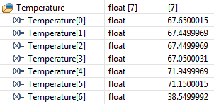
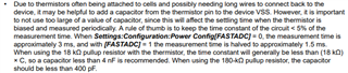
我们使用 BQ76952通过 使用 I2C  协议的 STM32进行电池管理、但遗憾 的是、我们无法获得热敏电阻的实际温度。 我们使用18k 热敏电阻(室温下为10k)。 我们在 TS1、TS3、HDQ、CFETOFF、DDSG 和 DCHG 引脚上连接6个热敏电阻。 但我们得到的值不准确。 在温度偏移(TS1TempOffset、CFETOFFTempOffset、TS3TempOffset、HDQTempOffset、DCHGTempOffset、 DDSGTempOffset)我们在每个热敏电阻上获得平均值70°C。 但实际温度应接近30°C

内部温度显示正确(内部温度0x68)。  

请帮助解决此问题。  正在寻找积极的回复。

此致、

Subhrajit Majumder。

  • 请注意,本文内容源自机器翻译,可能存在语法或其它翻译错误,仅供参考。如需获取准确内容,请参阅链接中的英语原文或自行翻译。

    Subhrajit、您好!

    您是否使用了 BQ769x2热敏电阻系数计算器来更新所选热敏电阻的系数? 该工具和说明位于以下位置: https://www.ti.com/tool/BQ769X2-THERMISTOR-COEFF-CALCULATOR

    此致、

    Matt

  • 请注意,本文内容源自机器翻译,可能存在语法或其它翻译错误,仅供参考。如需获取准确内容,请参阅链接中的英语原文或自行翻译。

    尊敬的 Matt:

    在 thermistors.txt 文件 How to find the registance value 中、我能否使用万用表测量寄存器。 在本例中、寄存器值为10k 欧姆。

    如何找到 温度(去油污)?  我是否需要指定 热敏电阻温度范围?

  • 请注意,本文内容源自机器翻译,可能存在语法或其它翻译错误,仅供参考。如需获取准确内容,请参阅链接中的英语原文或自行翻译。

    热敏电阻数据表应包含热敏电阻与温度的关系表。 您需要为您的热敏电阻找到该表。

  • 请注意,本文内容源自机器翻译,可能存在语法或其它翻译错误,仅供参考。如需获取准确内容,请参阅链接中的英语原文或自行翻译。

    非常感谢 Matt 的帮助。
    将很快更新结果。

    此致、

    Subhrajit Majumder。

  • 请注意,本文内容源自机器翻译,可能存在语法或其它翻译错误,仅供参考。如需获取准确内容,请参阅链接中的英语原文或自行翻译。

    尊敬的 Matt:  

    获得 系数后、我需要将值置于 TS1TempOffset、CFETOFFTempOffset、TS3TempOffset、HDQTempOffset、DCHGTempOffset、 为了获得更好的结果、DSGTempOffset?

  • 请注意,本文内容源自机器翻译,可能存在语法或其它翻译错误,仅供参考。如需获取准确内容,请参阅链接中的英语原文或自行翻译。

    这些系数进入 校准:18K 温度模型寄存器。 这应该在说明和器件 TRM 中进行解释。

  • 请注意,本文内容源自机器翻译,可能存在语法或其它翻译错误,仅供参考。如需获取准确内容,请参阅链接中的英语原文或自行翻译。

    尊敬的 Matt:

    共有10 个校准:18K 温度模型、如 校准:18K 温度模型:COEff A/ 校准:18K 温度模型:COEff b /校准:18K 温度模型:ADC0。

    我需要在哪个登记处设置系数?  

  • 请注意,本文内容源自机器翻译,可能存在语法或其它翻译错误,仅供参考。如需获取准确内容,请参阅链接中的英语原文或自行翻译。

    您是否收到了该工具的结果? 报告将告诉您需要输入的每个参数的参数和值。  

  • 请注意,本文内容源自机器翻译,可能存在语法或其它翻译错误,仅供参考。如需获取准确内容,请参阅链接中的英语原文或自行翻译。

    是的、先生。  

    我们得到了值、然后我们将其放置。 但没有区别。 我也连接了输出。

    ********
    搜索完成、bestmaxerr = 0.20000000000001705
    最佳 A [A1 A2 A3 A4 A5]=[-16669 31696 -27396 26324 1370]
    best B [B1 B2 B3 B4]=[-2110 3962-4296 4750]
    ADC0 = 11703
    *********

    我们从  BQ769x2热敏电阻系数计算器接收到的这些值。

    我还附加了我的代码、我将 系数 值放在这里。

    // 18k 温度模型
    BQ769x2_SetRegister (T18kCoeffa1、0xBEE3、2);// 18k Temp A1
    BQ769x2_SetRegister (T18kCoeffa2、0x7BD0、2);// 18k Temp A2
    BQ769x2_SetRegister (T18kCoeffa3、0x94FC、2);// 18k Temp A2
    BQ769x2_SetRegister (T18kCoeffa4、0x66D4、2);// 18k Temp A4
    BQ769x2_SetRegister (T18kCoeffa5、0x055A、2);// 18k Temp A5
    BQ769x2_SetRegister (T18kCoeffb1、0xF7C2、2);// 18k Temp B1
    BQ769x2_SetRegister (T18kCoeffb2、0x0F7A、2);// 18k Temp B2
    BQ769x2_SetRegister (T18kCoeffb3、0xEF38、2);// 18k Temp B3
    BQ769x2_SetRegister (T18kCoeffb4、0x128E、2);// 18k Temp b4
    BQ769x2_SetRegister (T18kAdc0、0x2DB7、2);// 18k ADC 0

  • 请注意,本文内容源自机器翻译,可能存在语法或其它翻译错误,仅供参考。如需获取准确内容,请参阅链接中的英语原文或自行翻译。

    我也附上我的代码...

    #include "main.h"
    #include "BQ769x2Header.h"
    /* Private includes ----------------------------------------------------------*/
    /* USER CODE BEGIN Includes */
    #define DEV_ADDR  0x10  // BQ769x2 address is 0x10 including R/W bit or 0x8 as 7-bit address
    #define CRC_Mode 1  // 0 for disabled, 1 for enabled
    #define MAX_BUFFER_SIZE 10
    #define R 0 // Read; Used in DirectCommands and Subcommands functions
    #define W 1 // Write; Used in DirectCommands and Subcommands functions
    #define W2 2 // Write data with two bytes; Used in Subcommands function
    uint8_t AFE_Flag= 1;
    HAL_StatusTypeDef res;
    /* USER CODE END Includes */
    
    /* Private typedef -----------------------------------------------------------*/
    /* USER CODE BEGIN PTD */
    
    /* USER CODE END PTD */
    
    /* Private define ------------------------------------------------------------*/
    /* USER CODE BEGIN PD */
    /* USER CODE END PD */
    
    /* Private macro -------------------------------------------------------------*/
    /* USER CODE BEGIN PM */
    
    /* USER CODE END PM */
    
    /* Private variables ---------------------------------------------------------*/
    I2C_HandleTypeDef hi2c2;
    
    TIM_HandleTypeDef htim16;
    
    /* USER CODE BEGIN PV */
    uint8_t RX_data [2] = {0x00, 0x00}; // used in several functions to store data read from BQ769x2
    uint8_t RX_2Byte [2] = {0x00, 0x00};
    uint8_t RX_3Byte [2] = {0x00, 0x00};
    uint8_t RX_4Byte [2] = {0x00, 0x00};
    uint8_t RX_5Byte [2] = {0x00, 0x00};
    uint32_t I_amp = 0x0000;
    uint8_t RX_32Byte [32] = {0x00, 0x00, 0x00, 0x00, 0x00, 0x00, 0x00, 0x00, 0x00, 0x00, 0x00, 0x00, 0x00, 0x00, 0x00, 0x00,
    	0x00, 0x00, 0x00, 0x00, 0x00, 0x00, 0x00, 0x00, 0x00, 0x00, 0x00, 0x00, 0x00, 0x00, 0x00, 0x00};
    	//used in Subcommands read function
    // Global Variables for cell voltages, temperatures, Stack voltage, PACK Pin voltage, LD Pin voltage, CC2 current
    uint16_t CellVoltage [16] = {0x00,0x00,0x00,0x00,0x00,0x00,0x00,0x00,0x00,0x00,0x00,0x00,0x00,0x00,0x00,0x00};
    float Temperature [7] = {0,0,0,0,0,0,0};
    uint16_t Stack_Voltage = 0x00;
    uint16_t Pack_Voltage = 0x00;
    uint16_t LD_Voltage = 0x00;
    int Pack_Current;
    int lc;
    uint16_t current = 0x00;
    
    uint16_t AlarmBits = 0x00;
    uint8_t value_SafetyAlertA;  // Safety Status Register A
    uint8_t value_SafetyAlertB;  // Safety Status Register B
    uint8_t value_SafetyAlertC;  // Safety Status Register C
    uint8_t value_SafetyStatusA;  // Safety Status Register A
    uint8_t value_SafetyStatusB;  // Safety Status Register B
    uint8_t value_SafetyStatusC;  // Safety Status Register C
    uint8_t value_PFStatusA;   // Permanent Fail Status Register A
    uint8_t value_PFStatusB;   // Permanent Fail Status Register B
    uint8_t value_PFStatusC;   // Permanent Fail Status Register C
    uint8_t FET_Status;  // FET Status register contents  - Shows states of FETs
    uint8_t value_FETOptions; //PreDischarge status
    uint16_t CB_ActiveCells;  // Cell Balancing Active Cells
    
    uint8_t	UV_Fault = 0;   // under-voltage fault state
    uint8_t	OV_Fault = 0;   // over-voltage fault state
    uint8_t	SCD_Fault = 0;  // short-circuit fault state
    uint8_t	OCD_Fault = 0;  // over-current fault state
    uint8_t	OCD_Fault1 = 0;
    uint8_t	OCC_Fault = 0;
    uint8_t ProtectionsTriggered = 0; // Set to 1 if any protection triggers
    
    uint8_t LD_ON = 0;	// Load Detect status bit
    uint8_t DSG = 0;   // discharge FET state
    uint8_t CHG = 0;   // charge FET state
    uint8_t PCHG = 0;  // pre-charge FET state
    uint8_t PDSG = 0;  // pre-discharge FET state
    uint8_t DCHG_pin = 0;
    uint8_t DDSG_pin = 0;
    uint8_t ALRT_pin = 0;
    uint8_t RSVD_pin = 0;
    
    uint8_t RSVD_00 = 0;
    uint8_t RSVD_01 = 0;
    uint8_t FET_INIT_OFF = 0;
    uint8_t PDSG_EN = 0;
    uint8_t FET_CTRL_EN = 0;
    uint8_t HOST_FET_EN = 0;
    uint8_t SLEEPCHG = 0;
    uint8_t SFET = 0;
    
    uint32_t CC1; // in BQ769x2_READPASSQ func
    uint32_t CC2;// in BQ769x2_READPASSQ func
    uint32_t CC3;// in BQ769x2_READPASSQ func
    uint32_t AccumulatedCharge_Int; // in BQ769x2_READPASSQ func
    uint32_t AccumulatedCharge_Frac;// in BQ769x2_READPASSQ func
    uint32_t AccumulatedCharge_Time;// in BQ769x2_READPASSQ func
    
    /* USER CODE END PV */
    
    /* Private function prototypes -----------------------------------------------*/
    void SystemClock_Config(void);
    static void MX_GPIO_Init(void);
    static void MX_I2C2_Init(void);
    static void MX_TIM16_Init(void);
    /* USER CODE BEGIN PFP */
    void delayUS(uint32_t us){
    	__HAL_TIM_SET_COUNTER(&htim16,0);  // set the counter value a 0
    		while (__HAL_TIM_GET_COUNTER(&htim16) < us);// wait for the counter to reach the us input in the parameter
    }
    
    void CopyArray(uint8_t *source, uint8_t *dest, uint8_t count)
    {
        uint8_t copyIndex = 0;
        for (copyIndex = 0; copyIndex < count; copyIndex++)
        {
            dest[copyIndex] = source[copyIndex];
        }
    }
    
    unsigned char Checksum(unsigned char *ptr, unsigned char len)
    // Calculates the checksum when writing to a RAM register. The checksum is the inverse of the sum of the bytes.
    {
    	unsigned char i;
    	unsigned char checksum = 0;
    
    	for(i=0; i<len; i++)
    		checksum += ptr[i];
    
    	checksum = 0xff & ~checksum;
    
    	return(checksum);
    }
    
    unsigned char CRC8(unsigned char *ptr, unsigned char len)
    //Calculates CRC8 for passed bytes. Used in i2c read and write functions
    {
    	unsigned char i;
    	unsigned char crc=0;
    	while(len--!=0)
    	{
    		for(i=0x80; i!=0; i/=2)
    		{
    			if((crc & 0x80) != 0)
    			{
    				crc *= 2;
    				crc ^= 0x107;
    			}
    			else
    				crc *= 2;
    
    			if((*ptr & i)!=0)
    				crc ^= 0x107;
    		}
    		ptr++;
    	}
    	return(crc);
    }
    
    void I2C_WriteReg(uint8_t reg_addr, uint8_t *reg_data, uint8_t count)
    {
    	uint8_t TX_Buffer [MAX_BUFFER_SIZE] = {0x00,0x00,0x00,0x00,0x00,0x00,0x00,0x00,0x00,0x00};
    #if CRC_Mode
    	{
    		uint8_t crc_count = 0;
    		crc_count = count * 2;
    		uint8_t crc1stByteBuffer [3] = {0x10, reg_addr, reg_data[0]};
    		unsigned int j;
    		unsigned int i;
    		uint8_t temp_crc_buffer [3];
    
    		TX_Buffer[0] = reg_data[0];
    		TX_Buffer[1] = CRC8(crc1stByteBuffer,3);
    
    
    		j = 2;
    		for(i=1; i<count; i++)
    		{
    			TX_Buffer[j] = reg_data[i];
    			j = j + 1;
    			temp_crc_buffer[0] = reg_data[i];
    			TX_Buffer[j] = CRC8(temp_crc_buffer,1);
    			j = j + 1;
    		}
    		HAL_I2C_Mem_Write(&hi2c2, DEV_ADDR, reg_addr, 1, TX_Buffer, crc_count, 1000);
    	}
    #else
    	HAL_I2C_Mem_Write(&hi2c2, 0x10<<1, reg_addr, 1, reg_data, count, 1000);
    #endif
    }
    unsigned int RX_CRC_Fail = 0;  // reset to 0. If in CRC Mode and CRC fails, this will be incremented.
    void I2C_ReadReg(uint8_t reg_addr, uint8_t *reg_data, uint8_t count)
    {
    //	unsigned int RX_CRC_Fail = 0;  // reset to 0. If in CRC Mode and CRC fails, this will be incremented.
    	uint8_t RX_Buffer [MAX_BUFFER_SIZE] = {0x00,0x00,0x00,0x00,0x00,0x00,0x00,0x00,0x00,0x00};
    #if CRC_Mode
    	{
    		uint8_t crc_count = 0;
    		uint8_t ReceiveBuffer [10] = {0x00,0x00,0x00,0x00,0x00,0x00,0x00,0x00,0x00,0x00};
    		crc_count = count * 2;
    		unsigned int j;
    		unsigned int i;
    		unsigned char CRCc = 0;
    		uint8_t temp_crc_buffer [3];
    
    		HAL_I2C_Mem_Read(&hi2c2, DEV_ADDR, reg_addr, 1, ReceiveBuffer, crc_count, 1000);
    		uint8_t crc1stByteBuffer [4] = {0x10, reg_addr, 0x11, ReceiveBuffer[0]};
    		CRCc = CRC8(crc1stByteBuffer,4);
    		if (CRCc != ReceiveBuffer[1])
    		{
    			RX_CRC_Fail += 1;
    		}
    		RX_Buffer[0] = ReceiveBuffer[0];
    
    		j = 2;
    		for (i=1; i<count; i++)
    		{
    			RX_Buffer[i] = ReceiveBuffer[j];
    			temp_crc_buffer[0] = ReceiveBuffer[j];
    			j = j + 1;
    			CRCc = CRC8(temp_crc_buffer,1);
    			if (CRCc != ReceiveBuffer[j])
    				RX_CRC_Fail += 1;
    			j = j + 1;
    		}
    		CopyArray(RX_Buffer, reg_data, crc_count);
    	}
    #else
    	HAL_I2C_Mem_Read(&hi2c2, 0x11, reg_addr, 2, reg_data, count, 1000);
    //	HAL_I2C_Master_Receive(&hi2c4, DEV_ADDR, reg_addr, 2, HAL_MAX_DELAY);
    #endif
    	return 0;
    }
    void BQ769x2_SetRegister(uint16_t reg_addr, uint32_t reg_data, uint8_t datalen)
    {
    	uint8_t TX_Buffer[2] = {0x00, 0x00};
    	uint8_t TX_RegData[6] = {0x00, 0x00, 0x00, 0x00, 0x00, 0x00};
    
    	//TX_RegData in little endian format
    	TX_RegData[0] = reg_addr & 0xff;
    	TX_RegData[1] = (reg_addr >> 8) & 0xff;
    	TX_RegData[2] = reg_data & 0xff; //1st byte of data
    
    	switch(datalen)
        {
    		case 1: //1 byte datalength
          		I2C_WriteReg(0x3E, TX_RegData, 3);
    			delayUS(2000);
    			TX_Buffer[0] = Checksum(TX_RegData, 3);
    			TX_Buffer[1] = 0x05; //combined length of register address and data
          		I2C_WriteReg(0x60, TX_Buffer, 2); // Write the checksum and length
    			delayUS(2000);
    			break;
    		case 2: //2 byte datalength
    			TX_RegData[3] = (reg_data >> 8) & 0xff;
    			I2C_WriteReg(0x3E, TX_RegData, 4);
    			delayUS(2000);
    			TX_Buffer[0] = Checksum(TX_RegData, 4);
    			TX_Buffer[1] = 0x06; //combined length of register address and data
          		I2C_WriteReg(0x60, TX_Buffer, 2); // Write the checksum and length
    			delayUS(2000);
    			break;
    		case 4: //4 byte datalength, Only used for CCGain and Capacity Gain
    			TX_RegData[3] = (reg_data >> 8) & 0xff;
    			TX_RegData[4] = (reg_data >> 16) & 0xff;
    			TX_RegData[5] = (reg_data >> 24) & 0xff;
    			I2C_WriteReg(0x3E, TX_RegData, 6);
    			delayUS(2000);
    			TX_Buffer[0] = Checksum(TX_RegData, 6);
    			TX_Buffer[1] = 0x08; //combined length of register address and data
          		I2C_WriteReg(0x60, TX_Buffer, 2); // Write the checksum and length
    			delayUS(2000);
    			break;
        }
    }
    void CommandSubcommands(uint16_t command) //For Command only Subcommands
    // See the TRM or the BQ76952 header file for a full list of Command-only subcommands
    {	//For DEEPSLEEP/SHUTDOWN subcommand you will need to call this function twice consecutively
    
    	uint8_t TX_Reg[2] = {0x00, 0x00};
    
    	//TX_Reg in little endian format
    	TX_Reg[0] = command & 0xff;
    	TX_Reg[1] = (command >> 8) & 0xff;
    
    	I2C_WriteReg(0x3E,TX_Reg,2);
    	delayUS(2000);
    }
    void Subcommands(uint16_t command, uint16_t data, uint8_t type)
    // See the TRM or the BQ76952 header file for a full list of Subcommands
    {
    	//security keys and Manu_data writes dont work with this function (reading these commands works)
    	//max readback size is 32 bytes i.e. DASTATUS, CUV/COV snapshot
    	uint8_t TX_Reg[4] = {0x00, 0x00, 0x00, 0x00};
    	uint8_t TX_Buffer[2] = {0x00, 0x00};
    
    	//TX_Reg in little endian format
    	TX_Reg[0] = command & 0xff;
    	TX_Reg[1] = (command >> 8) & 0xff;
    
    	if (type == R) {//read
    		I2C_WriteReg(0x3E,TX_Reg,2);
    		delayUS(2000);
    		I2C_ReadReg(0x40, RX_32Byte, 32); //RX_32Byte is a global variable
    	}
    	else if (type == W) {
    		//FET_Control, REG12_Control
    		TX_Reg[2] = data & 0xff;
    		I2C_WriteReg(0x3E,TX_Reg,3);
    		delayUS(1000);
    		TX_Buffer[0] = Checksum(TX_Reg, 3);
    		TX_Buffer[1] = 0x05; //combined length of registers address and data
    		I2C_WriteReg(0x60, TX_Buffer, 2);
    		delayUS(1000);
    	}
    	else if (type == W2){ //write data with 2 bytes
    		//CB_Active_Cells, CB_SET_LVL
    		TX_Reg[2] = data & 0xff;
    		TX_Reg[3] = (data >> 8) & 0xff;
    		I2C_WriteReg(0x3E,TX_Reg,4);
    		delayUS(1000);
    		TX_Buffer[0] = Checksum(TX_Reg, 4);
    		TX_Buffer[1] = 0x06; //combined length of registers address and data
    		I2C_WriteReg(0x60, TX_Buffer, 2);
    		delayUS(1000);
    	}
    }
    void DirectCommands(uint8_t command, uint16_t data, uint8_t type)
    // See the TRM or the BQ76952 header file for a full list of Direct Commands
    {	//type: R = read, W = write
    	uint8_t TX_data[2] = {0x00, 0x00};
    
    	//little endian format
    	TX_data[0] = data & 0xff;
    	TX_data[1] = (data >> 8) & 0xff;
    
    	if (type == R) {//Read
    		I2C_ReadReg(command, RX_data, 2); //RX_data is a global variable
    		delayUS(2000);
    	}
    	if (type == W) {//write
        //Control_status, alarm_status, alarm_enable all 2 bytes long
    		I2C_WriteReg(command,TX_data,2);
    		delayUS(2000);
    	}
    }
    
    void BQ769x2_Init() {
    	// Configures all parameters in device RAM
    
    	// Enter CONFIGUPDATE mode (Subcommand 0x0090) - It is required to be in CONFIG_UPDATE mode to program the device RAM settings
    	// See TRM for full description of CONFIG_UPDATE mode
    	CommandSubcommands(SET_CFGUPDATE);
    
    	// After entering CONFIG_UPDATE mode, RAM registers can be programmed. When programming RAM, checksum and length must also be
    	// programmed for the change to take effect. All of the RAM registers are described in detail in the BQ769x2 TRM.
    	// An easier way to find the descriptions is in the BQStudio Data Memory screen. When you move the mouse over the register name,
    	// a full description of the register and the bits will pop up on the screen.
    
    	// 'Power Config' - 0x9234 = 0x2D80
    	// Setting the DSLP_LDO bit allows the LDOs to remain active when the device goes into Deep Sleep mode
      	// Set wake speed bits to 00 for best performance
    	BQ769x2_SetRegister(PowerConfig, 0x2C80, 2);
    	// 'REG0 Config' - set REG0_EN bit to enable pre-regulator
    	BQ769x2_SetRegister(REG0Config, 0x01, 1);
    
    	// 'REG12 Config' - Enable REG1 with 3.3V output (0x0D for 3.3V, 0x0F for 5V)
    	BQ769x2_SetRegister(REG12Config, 0x0D, 1);
    
    
    	BQ769x2_SetRegister(FETOptions, 0x1D, 1);
    
    	BQ769x2_SetRegister(ChgPumpControl, 0x01, 1);
    
    	// Set DFETOFF pin to control BOTH CHG and DSG FET - 0x92FB = 0x42 (set to 0x00 to disable)
    //	BQ769x2_SetRegister(DFETOFFPinConfig, 0x00, 1);
    	BQ769x2_SetRegister(DFETOFFPinConfig, 0x0B, 1);
    	BQ769x2_SetRegister(CFETOFFPinConfig, 0x0B, 1);
    	// Set up ALERT Pin - 0x92FC = 0x2A
    	// This configures the ALERT pin to drive high (REG1 voltage) when enabled.
    	// The ALERT pin can be used as an interrupt to the MCU when a protection has triggered or new measurements are available
    //	BQ769x2_SetRegister(ALERTPinConfig, 0x2A, 1);
    	BQ769x2_SetRegister(ALERTPinConfig, 0x0B, 1);
    
    	// Set TS1 to measure Cell Temperature - 0x92FD = 0x07
    	BQ769x2_SetRegister(TS1Config, 0x07, 1);
    
    	BQ769x2_SetRegister(TS2Config, 0x0B, 1);
    
    	// Set TS3 to measure FET Temperature - 0x92FF = 0x0F
    	BQ769x2_SetRegister(TS3Config, 0x0F, 2);
    	// Set Temperature OFFSET
    	BQ769x2_SetRegister(TS1TempOffset, 0x80, 1);
    	BQ769x2_SetRegister(CFETOFFTempOffset, 0x80, 1);
    	BQ769x2_SetRegister(TS3TempOffset, 0x80, 1);
    	BQ769x2_SetRegister(HDQTempOffset, 0x80, 1);
    	BQ769x2_SetRegister(DCHGTempOffset, 0x80, 1);
    	BQ769x2_SetRegister(DDSGTempOffset, 0x80, 1);
    
    
    	// Set HDQ to measure Cell Temperature - 0x9300 = 0x07
    	BQ769x2_SetRegister(HDQPinConfig, 0x0B, 1);  // No thermistor installed on EVM HDQ pin, so set to 0x00
    	BQ769x2_SetRegister(DCHGPinConfig, 0x0B, 1); // DCHG Pin set low
    	BQ769x2_SetRegister(DDSGPinConfig, 0x0B, 1); // DDSG Pin set low
    
    //	18k Temperature model
    //	BQ769x2_SetRegister(T18kCoeffa1, 0xBEE3, 2); // 18k Temp a1
    //	BQ769x2_SetRegister(T18kCoeffa2, 0x7BD0, 2); // 18k Temp a2
    //	BQ769x2_SetRegister(T18kCoeffa3, 0x94FC, 2); // 18k Temp a2
    //	BQ769x2_SetRegister(T18kCoeffa4, 0x66D4, 2); // 18k Temp a4
    //	BQ769x2_SetRegister(T18kCoeffa5, 0x055A, 2); // 18k Temp a5
    //	BQ769x2_SetRegister(T18kCoeffb1, 0xF7C2, 2); // 18k Temp b1
    //	BQ769x2_SetRegister(T18kCoeffb2, 0x0F7A, 2); // 18k Temp b2
    //	BQ769x2_SetRegister(T18kCoeffb3, 0xEF38, 2); // 18k Temp b3
    //	BQ769x2_SetRegister(T18kCoeffb4, 0x128E, 2); // 18k Temp b4
    //	BQ769x2_SetRegister(T18kAdc0, 0x2DB7, 2); // 18k ADC 0
    
    
    	//	18k Temperature model based on EVM
    		BQ769x2_SetRegister(T18kCoeffa1, 0xC35C, 2); // 18k Temp a1
    		BQ769x2_SetRegister(T18kCoeffa2, 0x6737, 2); // 18k Temp a2
    		BQ769x2_SetRegister(T18kCoeffa3, 0xA778, 2); // 18k Temp a2
    		BQ769x2_SetRegister(T18kCoeffa4, 0x70A2, 2); // 18k Temp a4
    		BQ769x2_SetRegister(T18kCoeffa5, 0x02A0, 2); // 18k Temp a5
    		BQ769x2_SetRegister(T18kCoeffb1, 0xFE8D, 2); // 18k Temp b1
    		BQ769x2_SetRegister(T18kCoeffb2, 0x02C4, 2); // 18k Temp b2
    		BQ769x2_SetRegister(T18kCoeffb3, 0xF256, 2); // 18k Temp b3
    		BQ769x2_SetRegister(T18kCoeffb4, 0x13BB, 2); // 18k Temp b4
    		BQ769x2_SetRegister(T18kAdc0, 0x2DB7, 2); // 18k ADC 0
    
    
    	// 'VCell Mode' - Enable 16 cells - 0x9304 = 0x0000; Writing 0x0000 sets the default of 16 cells
    
    
    	BQ769x2_SetRegister(VCellMode, 0x3FFF, 2);
    //	BQ769x2_SetRegister(FET_CONTROL, 0x1111, 2);
    
    	// Enable protections in 'Enabled Protections A' 0x9261 = 0xBC
    	// Enables SCD (short-circuit), OCD1 (over-current in discharge), OCC (over-current in charge),
    	// COV (over-voltage), CUV (under-voltage)
    //	BQ769x2_SetRegister(EnabledProtectionsA, 0xBC, 1);
    	BQ769x2_SetRegister(EnabledProtectionsA, 0xFC, 1);
    	// Enable all protections in 'Enabled Protections B' 0x9262 = 0xF7
    	// Enables OTF (over-temperature FET), OTINT (internal over-temperature), OTD (over-temperature in discharge),
    	// OTC (over-temperature in charge), UTINT (internal under-temperature), UTD (under-temperature in discharge), UTC (under-temperature in charge)
    //	0xF7
    	BQ769x2_SetRegister(EnabledProtectionsB, 0x00, 1);
    	BQ769x2_SetRegister(EnabledProtectionsC, 0xE6, 1);
    	BQ769x2_SetRegister(CHGFETProtectionsA, 0x98, 1);
    	BQ769x2_SetRegister(DSGFETProtectionsA, 0xE4, 1);
    	// 'Default Alarm Mask' - 0x..82 Enables the FullScan and ADScan bits, default value = 0xF800
    	BQ769x2_SetRegister(DefaultAlarmMask, 0xF882, 2);
    
    	// Set up Cell Balancing Configuration - 0x9335 = 0x03   -  Automated balancing while in Relax or Charge modes
    	// Also see "Cell Balancing with BQ769x2 Battery Monitors" document on ti.com
    //	BQ769x2_SetRegister(BalancingConfiguration, 0x03, 1);
    	BQ769x2_SetRegister(BalancingConfiguration, 0x00, 1);
    // Set up CUV (under-voltage) Threshold - 0x9275 = 0x31 (2479 mV)
    //		0x31 to dec *50.6
    	// CUV Threshold is this value multiplied by 50.6mV
    //	0x29 = 2.074 volt, //	0x20 = 1.619 volt, //	0x39 = 2.88, //	0x38 = 2.83 // 0x32 = 2.530 || 0x17 = 1.163
    //	0x3A = 2.934 volt, // 0x3E = 3.1372 volt
     	BQ769x2_SetRegister(CUVThreshold, 0x3E, 1);
    
    	// Set up COV (over-voltage) Threshold - 0x9278 = 0x55 (4301 mV)
    	// COV Threshold is this value multiplied by 50.6mV
    //	0x40 = 3.238 || 0x3F = 3.187 || 0x55 = 4.301  ||0x5B = 4.604 || 0x48 = 	3.643 Volts || 0x47 = 3.592
    	BQ769x2_SetRegister(COVThreshold, 0x5B, 1);
    
    	// Set up OCC (over-current in charge) Threshold - 0x9280 = 0x05 (10 mV = 10A across 1mOhm sense resistor) Units in 2mV
    	BQ769x2_SetRegister(CUVDelay, 0x01, 1);
    	BQ769x2_SetRegister(COVDelay, 0x01, 1);
    
    	BQ769x2_SetRegister(CUVRecoveryHysteresis, 0x02, 1);
    //	BQ769x2_SetRegister(COVRecoveryHysteresis, 0x02, 1);
    	BQ769x2_SetRegister(ProtectionsRecoveryTime, 0x05, 1);
    	///:Recovery:Time
    	BQ769x2_SetRegister(DAConfiguration, 0x05, 1);
    //	BQ769x2_SetRegister(DsgCurrentThreshold, 2000, 2);
    //	BQ769x2_SetRegister(ChgCurrentThreshold, 3000, 2);
    
    //	Safety over current discharge threshold.
    //	BQ769x2_SetRegister(SOCDThreshold, 0x2000, 2);
    //	BQ769x2_SetRegister(SOCDDelay, 0x01, 1);
    
    	// Set up OCC (over-current in charge) Threshold - 0x9280 = 0x05 (10 mV = 10A across 1mOhm sense resistor) Units in 2mV
    	//	0x05
    	BQ769x2_SetRegister(OCCThreshold, 0x02, 1);
    //	BQ769x2_SetRegister(OCCRecoveryThreshold, 0x044C, 2);
    	// Set up OCD1 Threshold - 0x9282 = 0x0A (20 mV = 20A across 1mOhm sense resistor) units of 2mV
    	BQ769x2_SetRegister(OCD1Threshold, 0x01, 1);
    //	BQ769x2_SetRegister(OCD2Threshold, 0x03, 1);
    
    	BQ769x2_SetRegister(OCD1Delay, 0x01, 1);
    	BQ769x2_SetRegister(OCDLRecoveryTime, 0x01, 1);
    	BQ769x2_SetRegister(CCGain, 0x40F23055, 4);
    //	BQ769x2_SetRegister(CapacityGain, 0x64, 1);
    //	BQ769x2_SetRegister(CoulombCounterOffsetSamples, 0xFA00, 2);
    //	BQ769x2_SetRegister(BoardOffset, 0xFA00, 2);
    //  Set up SCD Threshold - 0x9286 = 0x05 (100 mV = 100A across 1mOhm sense resistor)  0x05=100mV
    	BQ769x2_SetRegister(SCDThreshold, 0x04, 1);
    
    	// Set up SCD Delay - 0x9287 = 0x03 (30 us) Enabled with a delay of (value - 1) * 15 µs; min value of 1
    	BQ769x2_SetRegister(SCDDelay, 0x03, 1);
    
    	// Set up SCDL Latch Limit to 1 to set SCD recovery only with load removal 0x9295 = 0x01
    	// If this is not set, then SCD will recover based on time (SCD Recovery Time parameter).
    	BQ769x2_SetRegister(SCDLLatchLimit, 0x01, 1);
    
    	BQ769x2_SetRegister(FETStatus, 0x3F, 1);
    
    	BQ769x2_SetRegister(MfgStatusInit, 0x0010, 2);
    
    
    	BQ769x2_SetRegister(PrechargeStartVoltage, 0x0C80, 4);
    	BQ769x2_SetRegister(PrechargeStopVoltage, 0X0CE4, 4);
    //	BQ769x2_SetRegister(PredischargeStopDelta, 50, 2);
    	BQ769x2_SetRegister(PredischargeTimeout, 0xFF, 2);
    	// Exit CONFIGUPDATE mode  - Subcommand 0x0092
    	CommandSubcommands(EXIT_CFGUPDATE);
    }
    void BQ769x2_ReadFETStatus() {
    	// Read FET Status to see which FETs are enabled
    	DirectCommands(FETStatus, 0x00, R);
    	FET_Status = (RX_data[1]*256 + RX_data[0]);
    	DSG = ((0x4 & RX_data[0])>>2);// discharge FET state
      	CHG = (0x1 & RX_data[0]);// charge FET state
      	PCHG = ((0x2 & RX_data[0])>>1);// pre-charge FET state
      	PDSG = ((0x8 & RX_data[0])>>3);// pre-discharge FET state
      	DCHG_pin = ((0x16 & RX_data[0])>>4);
      	DDSG_pin = ((0x32 & RX_data[0])>>5);
      	ALRT_pin = ((0x64 & RX_data[0])>>6);
      	RSVD_pin = ((0x128 & RX_data[0])>>7);
    }
    void BQ769x2_ReadSafetyStatus() { //good example functions
    	// Read Safety Status A/B/C and find which bits are set
    	// This shows which primary protections have been triggered
    	DirectCommands(SafetyAlertA, 0x00, R);
    	value_SafetyAlertA = (RX_data[1]*256 + RX_data[0]);
    	DirectCommands(SafetyAlertB, 0x00, R);
    	value_SafetyAlertB = (RX_data[1]*256 + RX_data[0]);
    	DirectCommands(SafetyAlertC, 0x00, R);
    	value_SafetyAlertC = (RX_data[1]*256 + RX_data[0]);
    
    	DirectCommands(SafetyStatusA, 0x00, R);
    	value_SafetyStatusA = (RX_data[1]*256 + RX_data[0]);
    	//Example Fault Flags
    	UV_Fault = ((0x4 & RX_data[0])>>2);
    	OV_Fault = ((0x8 & RX_data[0])>>3);
    	OCC_Fault = ((0x16 & RX_data[0])>>4);
    	OCD_Fault1 = ((0x32 & RX_data[0])>>5);
    	OCD_Fault = ((0x64 & RX_data[0])>>6);
    	SCD_Fault = ((0x128 & RX_data[0])>>7);
    
    	DirectCommands(SafetyStatusB, 0x00, R);
    	value_SafetyStatusB = (RX_data[1]*256 + RX_data[0]);
    	DirectCommands(SafetyStatusC, 0x00, R);
    	value_SafetyStatusC = (RX_data[1]*256 + RX_data[0]);
    	if ((value_SafetyStatusA + value_SafetyStatusB + value_SafetyStatusC) > 1) {
    		ProtectionsTriggered = 1; }
    	else {
    		ProtectionsTriggered = 0; }
    }
    
    void statusread(){
    	DirectCommands(FETOptions, 0x00, R);
    	value_FETOptions = (RX_data[1]*256 + RX_data[0]);
    	SFET = ((0x1 & RX_data[0])>>0);
    	SLEEPCHG = ((0x2 & RX_data[0])>>1);
    	HOST_FET_EN = ((0x4 & RX_data[0])>>2);
    	FET_CTRL_EN = ((0x8 & RX_data[0])>>3);
    	PDSG_EN = ((0x16 & RX_data[0])>>4);
    	FET_INIT_OFF = ((0x32 & RX_data[0])>>5);
    	RSVD_01 = ((0x64 & RX_data[0])>>6);
    	RSVD_00 = ((0x128 & RX_data[0])>>7);
    }
    
    void BQ769x2_ReadPFStatus() {
    	// Read Permanent Fail Status A/B/C and find which bits are set
    	// This shows which permanent failures have been triggered
    	DirectCommands(PFStatusA, 0x00, R);
    	value_PFStatusA = (RX_data[1]*256 + RX_data[0]);
    	DirectCommands(PFStatusB, 0x00, R);
    	value_PFStatusB = (RX_data[1]*256 + RX_data[0]);
    	DirectCommands(PFStatusC, 0x00, R);
    	value_PFStatusC = (RX_data[1]*256 + RX_data[0]);
    }
    uint16_t BQ769x2_ReadAlarmStatus() {
    	// Read this register to find out why the ALERT pin was asserted
    	DirectCommands(AlarmStatus, 0x00, R);
    	return (RX_data[1]*256 + RX_data[0]);
    }
    
    uint16_t BQ769x2_ReadVoltage(uint8_t command)
    // This function can be used to read a specific cell voltage or stack / pack / LD voltage
    {
    	//RX_data is global var
    	DirectCommands(command, 0x00, R);
    	if(command >= Cell1Voltage && command <= Cell16Voltage) {//Cells 1 through 16 (0x14 to 0x32)
    		return (RX_data[1]*256 + RX_data[0]); //voltage is reported in mV
    	}
    	else {//stack, Pack, LD
    		return 10 * (RX_data[1]*256 + RX_data[0]); //voltage is reported in 0.01V units
    	}
    
    }
    void BQ769x2_ReadAllVoltages()
    // Reads all cell voltages, Stack voltage, PACK pin voltage, and LD pin voltage
    {
      int cellvoltageholder = Cell1Voltage; //Cell1Voltage is 0x14
      for (int x = 0; x < 16; x++){//Reads all cell voltages
        CellVoltage[x] = BQ769x2_ReadVoltage(cellvoltageholder);
        cellvoltageholder = cellvoltageholder + 2;
      }
      Stack_Voltage = BQ769x2_ReadVoltage(StackVoltage);
      Pack_Voltage = BQ769x2_ReadVoltage(PACKPinVoltage);
      LD_Voltage = BQ769x2_ReadVoltage(LDPinVoltage);
    }
    uint16_t BQ769x2_ReadCurrent()
    // Reads PACK current
    {
    	DirectCommands(CC2Current, 0x00, R);
    	return (RX_data[1]*256 + RX_data[0]);  // current is reported in mA
    }
    uint16_t AFE_ReadCurrent() {
    	I2C_ReadReg(0x3A, RX_2Byte, 2);
    	return (RX_2Byte[1]*256 + RX_2Byte[0]);  // current is reported in mA
    }
    float BQ769x2_ReadTemperature(uint8_t command)
    {
    	DirectCommands(command, 0x00, R);
    	//RX_data is a global var
    	return (0.1 * (float)(RX_data[1]*256 + RX_data[0])) - 273.15;  // converts from 0.1K to Celcius
    }
    
    /* USER CODE END PFP */
    
    /* Private user code ---------------------------------------------------------*/
    /* USER CODE BEGIN 0 */
    
    /* USER CODE END 0 */
    
    /**
      * @brief  The application entry point.
      * @retval int
      */
    int main(void)
    {
      /* USER CODE BEGIN 1 */
    
      /* USER CODE END 1 */
    
      /* MCU Configuration--------------------------------------------------------*/
    
      /* Reset of all peripherals, Initializes the Flash interface and the Systick. */
      HAL_Init();
    
      /* USER CODE BEGIN Init */
    
      /* USER CODE END Init */
    
      /* Configure the system clock */
      SystemClock_Config();
    
      /* USER CODE BEGIN SysInit */
    
      /* USER CODE END SysInit */
    
      /* Initialize all configured peripherals */
      MX_GPIO_Init();
      MX_I2C2_Init();
      MX_TIM16_Init();
      /* USER CODE BEGIN 2 */
      HAL_TIM_Base_Start(&htim16);
    
      	HAL_GPIO_WritePin(GPIOA, GPIO_PIN_9, GPIO_PIN_RESET);  // RST_SHUT pin set low
      	HAL_GPIO_WritePin(GPIOA, GPIO_PIN_8, GPIO_PIN_RESET);  // DFETOFF pin (BOTHOFF) set low
        	delayUS(10000);
    
      	CommandSubcommands(BQ769x2_RESET);  // Resets the BQ769x2 registers
      	delayUS(60000);
      	BQ769x2_Init();  // Configure all of the BQ769x2 register settings
      	delayUS(10000);
      	CommandSubcommands(FET_ENABLE); // Enable the CHG and DSG FETs
      	delayUS(10000);
      	CommandSubcommands(SLEEP_DISABLE); // Sleep mode is enabled by default. For this example, Sleep is disabled to
      									   // demonstrate full-speed measurements in Normal mode.
    
      	delayUS(60000); delayUS(60000); delayUS(60000); delayUS(60000);  //wait to start measurements after FETs close
      /* USER CODE END 2 */
    
      /* Infinite loop */
      /* USER CODE BEGIN WHILE */
      while (1)
      {
        /* USER CODE END WHILE */
    	  BQ769x2_ReadAllVoltages();
    	  Pack_Current = BQ769x2_ReadCurrent();
    	  BQ769x2_ReadFETStatus();
    	  statusread();
    	  BQ769x2_ReadSafetyStatus();
    	  BQ769x2_ReadPFStatus();
    	  BQ769x2_ReadFETStatus();
    	  Temperature[0] = BQ769x2_ReadTemperature(TS1Temperature);
    	  Temperature[1] = BQ769x2_ReadTemperature(CFETOFFTemperature);
    	  Temperature[2] = BQ769x2_ReadTemperature(TS3Temperature);
    	  Temperature[3] = BQ769x2_ReadTemperature(HDQTemperature);
    	  Temperature[4] = BQ769x2_ReadTemperature(DCHGTemperature);
    	  Temperature[5] = BQ769x2_ReadTemperature(DDSGTemperature);
    	  Temperature[6] = BQ769x2_ReadTemperature(IntTemperature);
    	  HAL_Delay(200);
        /* USER CODE BEGIN 3 */
      }
      /* USER CODE END 3 */
    }
    
    /**
      * @brief System Clock Configuration
      * @retval None
      */
    void SystemClock_Config(void)
    {
      RCC_OscInitTypeDef RCC_OscInitStruct = {0};
      RCC_ClkInitTypeDef RCC_ClkInitStruct = {0};
    
      /** Initializes the RCC Oscillators according to the specified parameters
      * in the RCC_OscInitTypeDef structure.
      */
      RCC_OscInitStruct.OscillatorType = RCC_OSCILLATORTYPE_HSI48;
      RCC_OscInitStruct.HSI48State = RCC_HSI48_ON;
      RCC_OscInitStruct.PLL.PLLState = RCC_PLL_NONE;
      if (HAL_RCC_OscConfig(&RCC_OscInitStruct) != HAL_OK)
      {
        Error_Handler();
      }
    
      /** Initializes the CPU, AHB and APB buses clocks
      */
      RCC_ClkInitStruct.ClockType = RCC_CLOCKTYPE_HCLK|RCC_CLOCKTYPE_SYSCLK
                                  |RCC_CLOCKTYPE_PCLK1;
      RCC_ClkInitStruct.SYSCLKSource = RCC_SYSCLKSOURCE_HSI48;
      RCC_ClkInitStruct.AHBCLKDivider = RCC_SYSCLK_DIV1;
      RCC_ClkInitStruct.APB1CLKDivider = RCC_HCLK_DIV1;
    
      if (HAL_RCC_ClockConfig(&RCC_ClkInitStruct, FLASH_LATENCY_1) != HAL_OK)
      {
        Error_Handler();
      }
    }
    
    /**
      * @brief I2C2 Initialization Function
      * @param None
      * @retval None
      */
    static void MX_I2C2_Init(void)
    {
    
      /* USER CODE BEGIN I2C2_Init 0 */
    
      /* USER CODE END I2C2_Init 0 */
    
      /* USER CODE BEGIN I2C2_Init 1 */
    
      /* USER CODE END I2C2_Init 1 */
      hi2c2.Instance = I2C2;
      hi2c2.Init.Timing = 0x9010DEFF;
      hi2c2.Init.OwnAddress1 = 0;
      hi2c2.Init.AddressingMode = I2C_ADDRESSINGMODE_7BIT;
      hi2c2.Init.DualAddressMode = I2C_DUALADDRESS_DISABLE;
      hi2c2.Init.OwnAddress2 = 0;
      hi2c2.Init.OwnAddress2Masks = I2C_OA2_NOMASK;
      hi2c2.Init.GeneralCallMode = I2C_GENERALCALL_DISABLE;
      hi2c2.Init.NoStretchMode = I2C_NOSTRETCH_ENABLE;
      if (HAL_I2C_Init(&hi2c2) != HAL_OK)
      {
        Error_Handler();
      }
    
      /** Configure Analogue filter
      */
      if (HAL_I2CEx_ConfigAnalogFilter(&hi2c2, I2C_ANALOGFILTER_ENABLE) != HAL_OK)
      {
        Error_Handler();
      }
    
      /** Configure Digital filter
      */
      if (HAL_I2CEx_ConfigDigitalFilter(&hi2c2, 0) != HAL_OK)
      {
        Error_Handler();
      }
      /* USER CODE BEGIN I2C2_Init 2 */
    
      /* USER CODE END I2C2_Init 2 */
    
    }
    
    /**
      * @brief TIM16 Initialization Function
      * @param None
      * @retval None
      */
    static void MX_TIM16_Init(void)
    {
    
      /* USER CODE BEGIN TIM16_Init 0 */
    	TIM_ClockConfigTypeDef sClockSourceConfig = {0};
    	  TIM_MasterConfigTypeDef sMasterConfig = {0};
      /* USER CODE END TIM16_Init 0 */
    
      /* USER CODE BEGIN TIM16_Init 1 */
    
      /* USER CODE END TIM16_Init 1 */
      htim16.Instance = TIM16;
      htim16.Init.Prescaler = 63;
      htim16.Init.CounterMode = TIM_COUNTERMODE_UP;
      htim16.Init.Period = 65535;
      htim16.Init.ClockDivision = TIM_CLOCKDIVISION_DIV1;
      htim16.Init.RepetitionCounter = 0;
      htim16.Init.AutoReloadPreload = TIM_AUTORELOAD_PRELOAD_DISABLE;
      if (HAL_TIM_Base_Init(&htim16) != HAL_OK)
      {
        Error_Handler();
      }
      /* USER CODE BEGIN TIM16_Init 2 */
      sClockSourceConfig.ClockSource = TIM_CLOCKSOURCE_INTERNAL;
         if (HAL_TIM_ConfigClockSource(&htim16, &sClockSourceConfig) != HAL_OK)
         {
           Error_Handler();
         }
         sMasterConfig.MasterOutputTrigger = TIM_TRGO_RESET;
         sMasterConfig.MasterSlaveMode = TIM_MASTERSLAVEMODE_DISABLE;
         if (HAL_TIMEx_MasterConfigSynchronization(&htim16, &sMasterConfig) != HAL_OK)
         {
           Error_Handler();
         }
      /* USER CODE END TIM16_Init 2 */
    
    }
    
    /**
      * @brief GPIO Initialization Function
      * @param None
      * @retval None
      */
    static void MX_GPIO_Init(void)
    {
      GPIO_InitTypeDef GPIO_InitStruct = {0};
    
      /* GPIO Ports Clock Enable */
      __HAL_RCC_GPIOC_CLK_ENABLE();
      __HAL_RCC_GPIOF_CLK_ENABLE();
      __HAL_RCC_GPIOB_CLK_ENABLE();
      __HAL_RCC_GPIOA_CLK_ENABLE();
    
      /*Configure GPIO pin Output Level */
      HAL_GPIO_WritePin(GPIOB, GPIO_PIN_3|GPIO_PIN_4|GPIO_PIN_5, GPIO_PIN_RESET);
    
      /*Configure GPIO pins : PB3 PB4 PB5 */
      GPIO_InitStruct.Pin = GPIO_PIN_3|GPIO_PIN_4|GPIO_PIN_5;
      GPIO_InitStruct.Mode = GPIO_MODE_OUTPUT_PP;
      GPIO_InitStruct.Pull = GPIO_NOPULL;
      GPIO_InitStruct.Speed = GPIO_SPEED_FREQ_LOW;
      HAL_GPIO_Init(GPIOB, &GPIO_InitStruct);
    
    }
    
    /* USER CODE BEGIN 4 */
    
    /* USER CODE END 4 */
    
    /**
      * @brief  This function is executed in case of error occurrence.
      * @retval None
      */
    void Error_Handler(void)
    {
      /* USER CODE BEGIN Error_Handler_Debug */
      /* User can add his own implementation to report the HAL error return state */
      __disable_irq();
      while (1)
      {
      }
      /* USER CODE END Error_Handler_Debug */
    }
    
    #ifdef  USE_FULL_ASSERT
    /**
      * @brief  Reports the name of the source file and the source line number
      *         where the assert_param error has occurred.
      * @param  file: pointer to the source file name
      * @param  line: assert_param error line source number
      * @retval None
      */
    void assert_failed(uint8_t *file, uint32_t line)
    {
      /* USER CODE BEGIN 6 */
      /* User can add his own implementation to report the file name and line number,
         ex: printf("Wrong parameters value: file %s on line %d\r\n", file, line) */
      /* USER CODE END 6 */
    }
    #endif /* USE_FULL_ASSERT */
    

  • 请注意,本文内容源自机器翻译,可能存在语法或其它翻译错误,仅供参考。如需获取准确内容,请参阅链接中的英语原文或自行翻译。

    Subhrajit、您好!

    这些设置看起来正确、我在电路板上测试了它们并看到了合理的结果。 除了热敏电阻(如并联串联电阻或电容器)之外、您的电路板上是否还有其他可能影响测量的组件?

    我确实注意到了一些不相关的东西。 您的 VCell_Mode 设置未使用顶部电池。 如果您观看原理图视频或查看数据表的未使用引脚部分- VC15和 VC16引脚之间应连接一个电芯-这些引脚不应短接在一起。 有关更多信息、请参阅此主题:

    https://e2e.ti.com/support/power-management-group/power-management/f/power-management-forum/1176908/faq-bq76952-connecting-battery-cells-to-the-bq769x2-family-of-monitors 

    此致、

    Matt

  • 请注意,本文内容源自机器翻译,可能存在语法或其它翻译错误,仅供参考。如需获取准确内容,请参阅链接中的英语原文或自行翻译。

    Subhrajit、您好!

    您将问题标记为已解决-您是否介意分享导致读数不准确的原因。 这可能对将来的其他用户有所帮助。

    谢谢、此致、

    Matt

  • 请注意,本文内容源自机器翻译,可能存在语法或其它翻译错误,仅供参考。如需获取准确内容,请参阅链接中的英语原文或自行翻译。

    尊敬的 Matt:

    我们 并联了0.47uF (25v)电容器。 现在、我们将这些电容器替换为100nF。 它现在可以完美地工作。

    非常感谢您的指导。   

  • 请注意,本文内容源自机器翻译,可能存在语法或其它翻译错误,仅供参考。如需获取准确内容,请参阅链接中的英语原文或自行翻译。

    Subhrajit、您好!

    很高兴听到并感谢大家的分享。 您实际上应该将100nF 更改为小得多的值。 以下是数据表中的指导:

    此致、

    Matt  

  • 请注意,本文内容源自机器翻译,可能存在语法或其它翻译错误,仅供参考。如需获取准确内容,请参阅链接中的英语原文或自行翻译。

    尊敬的 Matt:  

    请为我在下面附加的上述主题提供帮助。

    e2e.ti.com/.../4443776