Other Parts Discussed in Thread: C2000WARE, LAUNCHXL-F280049C
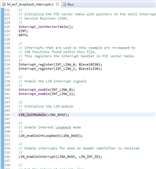
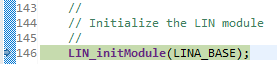
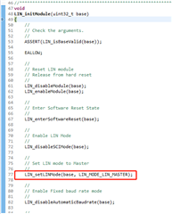
使用官方例程\C2000Ware_4_01_00_00\driverlib\f28004x\examples\lin\lin_ex1_loopback_interrupts进行调试
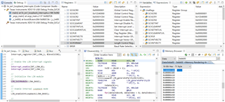
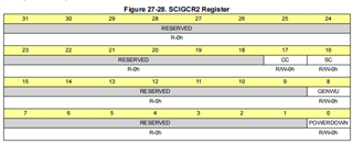
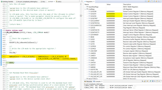
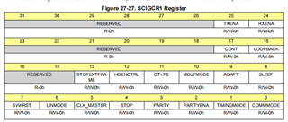
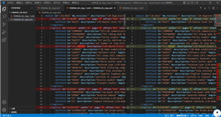
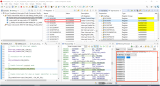
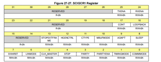
问题1:LIN寄存器显示的值与程序中的配置对不上,如下图SCIGCR1寄存器,被置1的位在手册上均为保留位
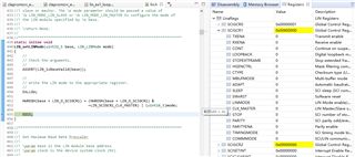
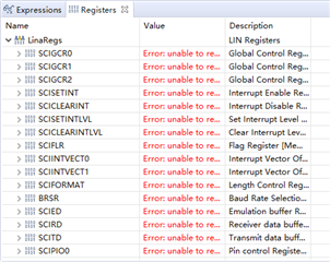
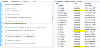
问题2:Memory Browser窗口内查看LIN寄存器地址内容无法显示

This thread has been locked.
If you have a related question, please click the "Ask a related question" button in the top right corner. The newly created question will be automatically linked to this question.
使用官方例程\C2000Ware_4_01_00_00\driverlib\f28004x\examples\lin\lin_ex1_loopback_interrupts进行调试
问题1:LIN寄存器显示的值与程序中的配置对不上,如下图SCIGCR1寄存器,被置1的位在手册上均为保留位
问题2:Memory Browser窗口内查看LIN寄存器地址内容无法显示

LIN 寄存器 xml 文件中的寄存器偏移量不正确。请使用附加的 xml 文件并将其替换在以下文件夹中:
<CCSInstallDir>\ccs\ccs_base\common\targetdb\Modules\C2000
f28004x_lin_regs.xml
<module id="LIN_REGS" HW_revision="" description="LIN Registers">
	<register id="SCIGCR0" width="32" page="1" offset="0x0" internal="0" description="Global Control Register 0">
		<bitfield id="RESET" description="LIN Module reset bit" begin="0" end="0" width="1" rwaccess="RW"/>
	</register>
	<register id="SCIGCR1" width="32" page="1" offset="0x2" internal="0" description="Global Control Register 1">
		<bitfield id="COMMMODE" description="SCI/LIN communications mode bit" begin="0" end="0" width="1" rwaccess="RW"/>
		<bitfield id="TIMINGMODE" description="SCI timing mode bit. Should be set to 1 for SCI mode." begin="1" end="1" width="1" rwaccess="RW"/>
		<bitfield id="PARITYENA" description="Parity enable" begin="2" end="2" width="1" rwaccess="RW"/>
		<bitfield id="PARITY" description="SCI parity odd/even selection" begin="3" end="3" width="1" rwaccess="RW"/>
		<bitfield id="STOP" description="SCI number of stop bits" begin="4" end="4" width="1" rwaccess="RW"/>
		<bitfield id="CLK_Master" description="LIN Master/Slave selection and SCI clock enable" begin="5" end="5" width="1" rwaccess="RW"/>
		<bitfield id="LINMODE" description="LIN Mode enable/disable" begin="6" end="6" width="1" rwaccess="RW"/>
		<bitfield id="SWnRST" description="Software reset" begin="7" end="7" width="1" rwaccess="RW"/>
		<bitfield id="SLEEP" description="SCI sleep (SCI compatibility mode)" begin="8" end="8" width="1" rwaccess="RW"/>
		<bitfield id="ADAPT" description="Automatic baudrate adjustment control(LIN mode)" begin="9" end="9" width="1" rwaccess="RW"/>
		<bitfield id="MBUFMODE" description="Multi-buffer mode" begin="10" end="10" width="1" rwaccess="RW"/>
		<bitfield id="CTYPE" description="Checksum type (LIN mode)" begin="11" end="11" width="1" rwaccess="RW"/>
		<bitfield id="HGENCTRL" description="Mask filtering comparison control (LIN mode)" begin="12" end="12" width="1" rwaccess="RW"/>
		<bitfield id="STOPEXTFRAME" description="Stop extended frame communication (LIN mode)" begin="13" end="13" width="1" rwaccess="RW"/>
		<bitfield id="LOOPBACK" description="Digital loopback mode" begin="16" end="16" width="1" rwaccess="RW"/>
		<bitfield id="CONT" description="Continue on suspend" begin="17" end="17" width="1" rwaccess="RW"/>
		<bitfield id="RXENA" description="Receive enable" begin="24" end="24" width="1" rwaccess="RW"/>
		<bitfield id="TXENA" description="Transmit enable" begin="25" end="25" width="1" rwaccess="RW"/>
	</register>
	<register id="SCIGCR2" width="32" page="1" offset="0x4" internal="0" description="Global Control Register 2">
		<bitfield id="POWERDOWN" description="Low-power mode PowerDown bit" begin="0" end="0" width="1" rwaccess="RW"/>
		<bitfield id="GENWU" description="Generate Wakeup" begin="8" end="8" width="1" rwaccess="RW"/>
		<bitfield id="SC" description="Send Checksum (LIN mode)" begin="16" end="16" width="1" rwaccess="RW"/>
		<bitfield id="CC" description="Compare Checksum (LIN mode)" begin="17" end="17" width="1" rwaccess="RW"/>
	</register>
	<register id="SCISETINT" width="32" page="1" offset="0x6" internal="0" description="Interrupt Enable Register">
		<bitfield id="SETBRKDTINT" description="Set Break-detect Interrupt (SCI compatible mode)" begin="0" end="0" width="1" rwaccess="RW"/>
		<bitfield id="SETWAKEUPINT" description="Set Wake-up Interrupt" begin="1" end="1" width="1" rwaccess="RW"/>
		<bitfield id="SETTIMEOUTINT" description="Set Timeout Interrupt (LIN only)" begin="4" end="4" width="1" rwaccess="RW"/>
		<bitfield id="SETTOAWUSINT" description="Set Timeout After Wakeup Signal Interrupt (LIN only)" begin="6" end="6" width="1" rwaccess="RW"/>
		<bitfield id="SETTOA3WUSINT" description="Set Timeout After 3 Wakeup Signals Interrupt (LIN only)" begin="7" end="7" width="1" rwaccess="RW"/>
		<bitfield id="SETTXINT" description="Set Transmitter Interrupt" begin="8" end="8" width="1" rwaccess="RW"/>
		<bitfield id="SETRXINT" description="Se Receiver Interrupt" begin="9" end="9" width="1" rwaccess="RW"/>
		<bitfield id="SETIDINT" description="Set Identifier Interrupt (LIN only)" begin="13" end="13" width="1" rwaccess="RW"/>
		<bitfield id="SET_TX_DMA" description="Set transmit DMA" begin="16" end="16" width="1" rwaccess="RW"/>
		<bitfield id="SET_RX_DMA" description="Set receiver DMA" begin="17" end="17" width="1" rwaccess="RW"/>
		<bitfield id="SET_RX_DMA_ALL" description="Set receiver DMA for Address and Data frames" begin="18" end="18" width="1" rwaccess="RW"/>
		<bitfield id="SETPEINT" description="Set Parity Interrupt" begin="24" end="24" width="1" rwaccess="RW"/>
		<bitfield id="SETOEINT" description="Set Overrun-Error Interrupt" begin="25" end="25" width="1" rwaccess="RW"/>
		<bitfield id="SETFEINT" description="Set Framing-Error Interrupt" begin="26" end="26" width="1" rwaccess="RW"/>
		<bitfield id="SETNREINT" description="Set No-Response-Error Interrupt (LIN only)" begin="27" end="27" width="1" rwaccess="RW"/>
		<bitfield id="SETISFEINT" description="Set Inconsistent-Sync-Field-Error Interrupt (LIN only)" begin="28" end="28" width="1" rwaccess="RW"/>
		<bitfield id="SETCEINT" description="Set Checksum-error Interrupt (LIN only)" begin="29" end="29" width="1" rwaccess="RW"/>
		<bitfield id="SETPBEINT" description="Set Physical Bus Error Interrupt (LIN only)" begin="30" end="30" width="1" rwaccess="RW"/>
		<bitfield id="SETBEINT" description="Set Bit Error Interrupt (LIN only)" begin="31" end="31" width="1" rwaccess="RW"/>
	</register>
	<register id="SCICLEARINT" width="32" page="1" offset="0x8" internal="0" description="Interrupt Disable Register">
		<bitfield id="CLRBRKDTINT" description="Clear Break-detect Interrupt (SCI compatible mode" begin="0" end="0" width="1" rwaccess="RW"/>
		<bitfield id="CLRWAKEUPINT" description="Clear Wake-up Interrupt" begin="1" end="1" width="1" rwaccess="RW"/>
		<bitfield id="CLRTIMEOUTINT" description="Clear Timeout Interrupt (LIN only)" begin="4" end="4" width="1" rwaccess="RW"/>
		<bitfield id="CLRTOAWUSINT" description="Clear Timeout After Wakeup Signal Interrupt (LIN only)" begin="6" end="6" width="1" rwaccess="RW"/>
		<bitfield id="CLRTOA3WUSINT" description="Clear Timeout After 3 Wakeup Signals Interrupt (LIN only)" begin="7" end="7" width="1" rwaccess="RW"/>
		<bitfield id="CLRTXINT" description="Clear Transmitter Interrupt" begin="8" end="8" width="1" rwaccess="RW"/>
		<bitfield id="CLRRXINT" description="Clear Receiver Interrupt" begin="9" end="9" width="1" rwaccess="RW"/>
		<bitfield id="CLRIDINT" description="Clear Identifier Interrupt (LIN only)" begin="13" end="13" width="1" rwaccess="RW"/>
		<bitfield id="CLRTXDMA" description="Clear transmit DMA" begin="16" end="16" width="1" rwaccess="RW"/>
		<bitfield id="SETRXDMA" description="Clear receiver DMA" begin="17" end="17" width="1" rwaccess="RW"/>
		<bitfield id="CLRPEINT" description="Clear Parity Interrupt" begin="24" end="24" width="1" rwaccess="RW"/>
		<bitfield id="CLROEINT" description="Clear Overrun-Error Interrupt" begin="25" end="25" width="1" rwaccess="RW"/>
		<bitfield id="CLRFEINT" description="Clear Framing-Error Interrupt" begin="26" end="26" width="1" rwaccess="RW"/>
		<bitfield id="CLRNREINT" description="Clear No-Response-Error Interrupt (LIN only)" begin="27" end="27" width="1" rwaccess="RW"/>
		<bitfield id="CLRISFEINT" description="Clear Inconsistent-Sync-Field-Error Interrupt (LIN only)" begin="28" end="28" width="1" rwaccess="RW"/>
		<bitfield id="CLRCEINT" description="Clear Checksum-error Interrupt (LIN only)" begin="29" end="29" width="1" rwaccess="RW"/>
		<bitfield id="CLRPBEINT" description="Clear Physical Bus Error Interrupt (LIN only)" begin="30" end="30" width="1" rwaccess="RW"/>
		<bitfield id="CLRBEINT" description="Clear Bit Error Interrupt (LIN only)" begin="31" end="31" width="1" rwaccess="RW"/>
	</register>
	<register id="SCISETINTLVL" width="32" page="1" offset="0xa" internal="0" description="Set Interrupt Level Register">
		<bitfield id="SETBRKDTINTLVL" description="Set Break-detect Interrupt Level (SCI compatible mode)" begin="0" end="0" width="1" rwaccess="RW"/>
		<bitfield id="SETWAKEUPINTLVL" description="Set Wake-up Interrupt Level" begin="1" end="1" width="1" rwaccess="RW"/>
		<bitfield id="SETTIMEOUTINTLVL" description="Set Timeout Interrupt Level (LIN only)" begin="4" end="4" width="1" rwaccess="RW"/>
		<bitfield id="SETTOAWUSINTLVL" description="Set Timeout After Wakeup Signal Interrupt Level (LIN only)" begin="6" end="6" width="1" rwaccess="RW"/>
		<bitfield id="SETTOA3WUSINTLVL" description="Set Timeout After 3 Wakeup Signals Interrupt Level" begin="7" end="7" width="1" rwaccess="RW"/>
		<bitfield id="SETTXINTLVL" description="Set Transmitter Interrupt Level" begin="8" end="8" width="1" rwaccess="RW"/>
		<bitfield id="SETRXINTOVO" description="Receiver Interrupt Enable Level" begin="9" end="9" width="1" rwaccess="RW"/>
		<bitfield id="SETIDINTLVL" description="Set Identifier Interrupt Level (LIN only)" begin="13" end="13" width="1" rwaccess="RW"/>
		<bitfield id="SETPEINTLVL" description="Set Parity Interrupt Level" begin="24" end="24" width="1" rwaccess="RW"/>
		<bitfield id="SETOEINTLVL" description="Set Overrun-Error Interrupt Level" begin="25" end="25" width="1" rwaccess="RW"/>
		<bitfield id="SETFEINTLVL" description="Set Framing-Error Interrupt Level" begin="26" end="26" width="1" rwaccess="RW"/>
		<bitfield id="SETNREINTLVL" description="Set No-Response-Error Interrupt Level (LIN only)" begin="27" end="27" width="1" rwaccess="RW"/>
		<bitfield id="SETISFEINTLVL" description="Set Inconsistent-Sync-Field-Error Interrupt Level" begin="28" end="28" width="1" rwaccess="RW"/>
		<bitfield id="SETCEINTLVL" description="Set Checksum-error Interrupt Level (LIN only)" begin="29" end="29" width="1" rwaccess="RW"/>
		<bitfield id="SETPBEINTLVL" description="Set Physical Bus Error Interrupt Level (LIN only)" begin="30" end="30" width="1" rwaccess="RW"/>
		<bitfield id="SETBEINTLVL" description="Set Bit Error Interrupt Level (LIN only)" begin="31" end="31" width="1" rwaccess="RW"/>
	</register>
	<register id="SCICLEARINTLVL" width="32" page="1" offset="0xc" internal="0" description="Clear Interrupt Level Register">
		<bitfield id="CLRBRKDTINTLVL" description="Clear Break-detect Interrupt Level (SCI compatible mode)" begin="0" end="0" width="1" rwaccess="RW"/>
		<bitfield id="CLRWAKEUPINTLVL" description="Clear Wake-up Interrupt Level" begin="1" end="1" width="1" rwaccess="RW"/>
		<bitfield id="CLRTIMEOUTINTLVL" description=" Clear Timeout Interrupt Level (LIN only)" begin="4" end="4" width="1" rwaccess="RW"/>
		<bitfield id="CLRTOAWUSINTLVL" description="Clear Timeout After Wakeup Signal Interrupt Level (LIN only)" begin="6" end="6" width="1" rwaccess="RW"/>
		<bitfield id="CLRTOA3WUSINTLVL" description="Clear Timeout After 3 Wakeup Signals" begin="7" end="7" width="1" rwaccess="RW"/>
		<bitfield id="CLRTXINTLVL" description="Clear Transmitter Interrupt Level" begin="8" end="8" width="1" rwaccess="RW"/>
		<bitfield id="CLRRXINTLVL" description="Clear Receiver interrupt Level." begin="9" end="9" width="1" rwaccess="RW"/>
		<bitfield id="CLRIDINTLVL" description="Clear Identifier Interrupt Level (LIN only)" begin="13" end="13" width="1" rwaccess="RW"/>
		<bitfield id="CLRPEINTLVL" description="Clear Parity Interrupt Level" begin="24" end="24" width="1" rwaccess="RW"/>
		<bitfield id="CLROEINTLVL" description="Clear Overrun-Error Interrupt Level" begin="25" end="25" width="1" rwaccess="RW"/>
		<bitfield id="CLRFEINTLVL" description="Clear Framing-Error Interrupt Level" begin="26" end="26" width="1" rwaccess="RW"/>
		<bitfield id="CLRNREINTLVL" description="Clear No-Response-Error Interrupt Level (LIN only)" begin="27" end="27" width="1" rwaccess="RW"/>
		<bitfield id="CLRISFEINTLVL" description="Clear Inconsistent-Sync-Field-Error" begin="28" end="28" width="1" rwaccess="RW"/>
		<bitfield id="CLRCEINTLVL" description="Clear Checksum-error Interrupt Level (LIN only)" begin="29" end="29" width="1" rwaccess="RW"/>
		<bitfield id="CLRPBEINTLVL" description="Clear Physical Bus Error Interrupt Level (LIN only)" begin="30" end="30" width="1" rwaccess="RW"/>
		<bitfield id="CLRBEINTLVL" description="Clear Bit Error Interrupt Level (LIN only)" begin="31" end="31" width="1" rwaccess="RW"/>
	</register>
	<register id="SCIFLR" width="32" page="1" offset="0xe" internal="0" description="Flag Register">
		<bitfield id="BRKDT" description="Break-detect Flag (SCI compatible mode)" begin="0" end="0" width="1" rwaccess="RW"/>
		<bitfield id="WAKEUP" description="Wake-up Flag" begin="1" end="1" width="1" rwaccess="RW"/>
		<bitfield id="IDLE" description="SCI receiver in idle state (SCI compatible mode)" begin="2" end="2" width="1" rwaccess="R"/>
		<bitfield id="BUSY" description="Busy Flag" begin="3" end="3" width="1" rwaccess="R"/>
		<bitfield id="TIMEOUT" description="LIN Bus IDLE timeout Flag (LIN only)" begin="4" end="4" width="1" rwaccess="RW"/>
		<bitfield id="TOAWUS" description="Timeout After Wakeup Signal Flag (LIN only)" begin="6" end="6" width="1" rwaccess="RW"/>
		<bitfield id="TOA3WUS" description="Timeout After 3 Wakeup Signals Flag (LIN only)" begin="7" end="7" width="1" rwaccess="RW"/>
		<bitfield id="TXRDY" description="Transmitter Buffer Ready Flag" begin="8" end="8" width="1" rwaccess="R"/>
		<bitfield id="RXRDY" description="Receiver Buffer Ready Flag" begin="9" end="9" width="1" rwaccess="RW"/>
		<bitfield id="TXWAKE" description="SCI Transmitter Wakeup Method Select" begin="10" end="10" width="1" rwaccess="RW"/>
		<bitfield id="TXEMPTY" description="Transmitter Empty Flag" begin="11" end="11" width="1" rwaccess="R"/>
		<bitfield id="RXWAKE" description="Receiver Wakeup Detect Flag" begin="12" end="12" width="1" rwaccess="R"/>
		<bitfield id="IDTXFLAG" description="Identifier On Transmit Flag (LIN only)" begin="13" end="13" width="1" rwaccess="RW"/>
		<bitfield id="IDRXFLAG" description="Identifier on Receive Flag" begin="14" end="14" width="1" rwaccess="RW"/>
		<bitfield id="PE" description="Parity Error Flag" begin="24" end="24" width="1" rwaccess="RW"/>
		<bitfield id="OE" description="Overrun Error Flag" begin="25" end="25" width="1" rwaccess="RW"/>
		<bitfield id="FE" description="Framing Error Flag" begin="26" end="26" width="1" rwaccess="RW"/>
		<bitfield id="NRE" description="No-Response Error Flag (LIN only)" begin="27" end="27" width="1" rwaccess="RW"/>
		<bitfield id="ISFE" description="Inconsistent Sync Field Error Flag (LIN only)" begin="28" end="28" width="1" rwaccess="RW"/>
		<bitfield id="CE" description="Checksum Error Flag (LIN only)" begin="29" end="29" width="1" rwaccess="RW"/>
		<bitfield id="PBE" description="Physical Bus Error Flag (LIN only)" begin="30" end="30" width="1" rwaccess="RW"/>
		<bitfield id="BE" description="Bit Error Flag (LIN only)" begin="31" end="31" width="1" rwaccess="RW"/>
	</register>
	<register id="SCIINTVECT0" width="32" page="1" offset="0x10" internal="0" description="Interrupt Vector Offset Register 0">
		<bitfield id="INTVECT0" description="LIN Module reset bit" begin="4" end="0" width="5" rwaccess="R"/>
	</register>
	<register id="SCIINTVECT1" width="32" page="1" offset="0x12" internal="0" description="Interrupt Vector Offset Register 1">
		<bitfield id="INTVECT1" description="LIN Module reset bit" begin="4" end="0" width="5" rwaccess="R"/>
	</register>
	<register id="SCIFORMAT" width="32" page="1" offset="0x14" internal="0" description="Length Control Register">
		<bitfield id="CHAR" description="Character Length Control Bits" begin="2" end="0" width="3" rwaccess="RW"/>
		<bitfield id="LENGTH" description="Frame Length Control Bits" begin="18" end="16" width="3" rwaccess="RW"/>
	</register>
	<register id="BRSR" width="32" page="1" offset="0x16" internal="0" description="Baud Rate Selection Register">
		<bitfield id="SCI_LIN_PSL" description="24-Bit Integer Prescaler Select (Low Bits)" begin="15" end="0" width="16" rwaccess="RW"/>
		<bitfield id="SCI_LIN_PSH" description="24-Bit Integer Prescaler Select (High Bits)" begin="23" end="16" width="8" rwaccess="RW"/>
		<bitfield id="M" description="M 4-bit Fractional Divider selection" begin="27" end="24" width="4" rwaccess="RW"/>
		<bitfield id="U" description="U Superfractional divider Selection" begin="30" end="28" width="3" rwaccess="RW"/>
	</register>
	<register id="SCIED" width="32" page="1" offset="0x18" internal="0" description="Emulation buffer Register">
		<bitfield id="ED" description="Receiver Emulation Data." begin="7" end="0" width="8" rwaccess="R"/>
	</register>
	<register id="SCIRD" width="32" page="1" offset="0x1a" internal="0" description="Receiver data buffer Register">
		<bitfield id="RD" description="Received Data." begin="7" end="0" width="8" rwaccess="R"/>
	</register>
	<register id="SCITD" width="32" page="1" offset="0x1c" internal="0" description="Transmit data buffer Register">
		<bitfield id="TD" description="Transmit data" begin="7" end="0" width="8" rwaccess="RW"/>
	</register>
	<register id="SCIPIO0" width="32" page="1" offset="0x1e" internal="0" description="Pin control Register 0">
		<bitfield id="RXFUNC" description="LINRX pin function" begin="1" end="1" width="1" rwaccess="RW"/>
		<bitfield id="TXFUNC" description="LINTX pin function" begin="2" end="2" width="1" rwaccess="RW"/>
	</register>
	<register id="SCIPIO2" width="32" page="1" offset="0x22" internal="0" description="Pin control Register 2">
		<bitfield id="RXIN" description="SCIRX pin value" begin="1" end="1" width="1" rwaccess="R"/>
		<bitfield id="TXIN" description="SCITX pin value" begin="2" end="2" width="1" rwaccess="R"/>
	</register>
	<register id="LINCOMP" width="32" page="1" offset="0x30" internal="0" description="Compare register">
		<bitfield id="SBREAK" description="Sync Break Extend" begin="2" end="0" width="3" rwaccess="RW"/>
		<bitfield id="SDEL" description="Sync Delimiter Compare" begin="9" end="8" width="2" rwaccess="RW"/>
	</register>
	<register id="LINRD0" width="32" page="1" offset="0x32" internal="0" description="Receive data register 0">
		<bitfield id="RD3" description="Receive Buffer 3" begin="7" end="0" width="8" rwaccess="R"/>
		<bitfield id="RD2" description="Receive Buffer 2" begin="15" end="8" width="8" rwaccess="R"/>
		<bitfield id="RD1" description="Receive Buffer 1" begin="23" end="16" width="8" rwaccess="R"/>
		<bitfield id="RD0" description="Receive Buffer 0" begin="31" end="24" width="8" rwaccess="R"/>
	</register>
	<register id="LINRD1" width="32" page="1" offset="0x34" internal="0" description="Receive data register 1">
		<bitfield id="RD7" description="Receive Buffer 3" begin="7" end="0" width="8" rwaccess="R"/>
		<bitfield id="RD6" description="Receive Buffer 2" begin="15" end="8" width="8" rwaccess="R"/>
		<bitfield id="RD5" description="Receive Buffer 1" begin="23" end="16" width="8" rwaccess="R"/>
		<bitfield id="RD4" description="Receive Buffer 0" begin="31" end="24" width="8" rwaccess="R"/>
	</register>
	<register id="LINMASK" width="32" page="1" offset="0x36" internal="0" description="Acceptance mask register">
		<bitfield id="TXIDMASK" description="TX ID Mask bits (LIN only)" begin="7" end="0" width="8" rwaccess="RW"/>
		<bitfield id="RXIDMASK" description="RX ID Mask bits (LIN only)" begin="23" end="16" width="8" rwaccess="RW"/>
	</register>
	<register id="LINID" width="32" page="1" offset="0x38" internal="0" description="LIN ID Register">
		<bitfield id="IDBYTE" description="LIN message ID (LIN only)" begin="7" end="0" width="8" rwaccess="RW"/>
		<bitfield id="IDSLAVETASKBYTE" description="ID  Slave Task byte (LIN only)" begin="15" end="8" width="8" rwaccess="RW"/>
		<bitfield id="RECEIVEDID" description="Current Message ID (LIN only)" begin="23" end="16" width="8" rwaccess="R"/>
	</register>
	<register id="LINTD0" width="32" page="1" offset="0x3a" internal="0" description="Transmit Data Register 0">
		<bitfield id="TD3" description="TRANSMIT Buffer 3" begin="7" end="0" width="8" rwaccess="RW"/>
		<bitfield id="TD2" description="TRANSMIT Buffer 2" begin="15" end="8" width="8" rwaccess="RW"/>
		<bitfield id="TD1" description="TRANSMIT Buffer 1" begin="23" end="16" width="8" rwaccess="RW"/>
		<bitfield id="TD0" description="TRANSMIT Buffer 0" begin="31" end="24" width="8" rwaccess="RW"/>
	</register>
	<register id="LINTD1" width="32" page="1" offset="0x3c" internal="0" description="Transmit Data Register 1">
		<bitfield id="TD7" description="TRANSMIT Buffer 7" begin="7" end="0" width="8" rwaccess="RW"/>
		<bitfield id="TD6" description="TRANSMIT Buffer 6" begin="15" end="8" width="8" rwaccess="RW"/>
		<bitfield id="TD5" description="TRANSMIT Buffer 5" begin="23" end="16" width="8" rwaccess="RW"/>
		<bitfield id="TD4" description="TRANSMIT Buffer 4" begin="31" end="24" width="8" rwaccess="RW"/>
	</register>
	<register id="MBRSR" width="32" page="1" offset="0x3e" internal="0" description="Maximum Baud Rate Selection Register">
		<bitfield id="MBR" description="Received Data." begin="12" end="0" width="13" rwaccess="RW"/>
	</register>
	<register id="IODFTCTRL" width="32" page="1" offset="0x48" internal="0" description="IODFT for LIN">
		<bitfield id="RXPENA" description="Analog Loopback Via Receive Pin Enable" begin="0" end="0" width="1" rwaccess="RW"/>
		<bitfield id="LPBENA" description="Module Loopback Enable" begin="1" end="1" width="1" rwaccess="RW"/>
		<bitfield id="IODFTENA" description="IO DFT Enable Key" begin="11" end="8" width="4" rwaccess="RW"/>
		<bitfield id="TXSHIFT" description="Transmit Delay Shift" begin="18" end="16" width="3" rwaccess="RW"/>
		<bitfield id="PINSAMPLEMASK" description="TX Pin Sample Mask" begin="20" end="19" width="2" rwaccess="RW"/>
		<bitfield id="BRKDTERRENA" description="Break Detect Error Enable (SCI compatibility mode)" begin="24" end="24" width="1" rwaccess="RW"/>
		<bitfield id="PERRENA" description="Parity Error Enable (SCI compatibility mode)" begin="25" end="25" width="1" rwaccess="RW"/>
		<bitfield id="FERRENA" description="Frame Error Enable (SCI compatibility mode)" begin="26" end="26" width="1" rwaccess="RW"/>
		<bitfield id="ISFERRENA" description="Inconsistent Sync Field Error Enable (LIN mode)" begin="28" end="28" width="1" rwaccess="RW"/>
		<bitfield id="CERRENA" description="Checksum Error Enable(LIN mode)" begin="29" end="29" width="1" rwaccess="RW"/>
		<bitfield id="PBERRENA" description="Physical Bus Error Enable (LIN mode)" begin="30" end="30" width="1" rwaccess="RW"/>
		<bitfield id="BERRENA" description="Bit Error Enable (LIN mode)" begin="31" end="31" width="1" rwaccess="RW"/>
	</register>
	<register id="LIN_GLB_INT_EN" width="32" page="1" offset="0x70" internal="0" description="LIN Global Interrupt Enable Register">
		<bitfield id="GLBINT0_EN" description="Global Interrupt Enable for LIN INT0" begin="0" end="0" width="1" rwaccess="RW"/>
		<bitfield id="GLBINT1_EN" description="Global Interrupt Enable for LIN INT1" begin="1" end="1" width="1" rwaccess="RW"/>
	</register>
	<register id="LIN_GLB_INT_FLG" width="32" page="1" offset="0x72" internal="0" description="LIN Global Interrupt Flag Register">
		<bitfield id="INT0_FLG" description="Global Interrupt Flag for LIN INT0" begin="0" end="0" width="1" rwaccess="R"/>
		<bitfield id="INT1_FLG" description="Global Interrupt Flag for LIN INT1" begin="1" end="1" width="1" rwaccess="R"/>
	</register>
	<register id="LIN_GLB_INT_CLR" width="32" page="1" offset="0x74" internal="0" description="LIN Global Interrupt Clear Register">
		<bitfield id="INT0_FLG_CLR" description="Global Interrupt flag clear for LIN INT0" begin="0" end="0" width="1" rwaccess="RW"/>
		<bitfield id="INT1_FLG_CLR" description="Global Interrupt flag  clear for LIN INT1" begin="1" end="1" width="1" rwaccess="RW"/>
	</register>
</module>
试一下这个:
<module id="LIN_REGS" HW_revision="" description="LIN Registers">
	<register id="SCIGCR0" width="32" page="1" offset="0x0" internal="0" description="Global Control Register 0">
		<bitfield id="RESET" description="LIN Module reset bit" begin="0" end="0" width="1" rwaccess="RW"/>
	</register>
	<register id="SCIGCR1" width="32" page="1" offset="0x4" internal="0" description="Global Control Register 1">
		<bitfield id="COMMMODE" description="SCI/LIN communications mode bit" begin="0" end="0" width="1" rwaccess="RW"/>
		<bitfield id="TIMINGMODE" description="SCI timing mode bit. Should be set to 1 for SCI mode." begin="1" end="1" width="1" rwaccess="RW"/>
		<bitfield id="PARITYENA" description="Parity enable" begin="2" end="2" width="1" rwaccess="RW"/>
		<bitfield id="PARITY" description="SCI parity odd/even selection" begin="3" end="3" width="1" rwaccess="RW"/>
		<bitfield id="STOP" description="SCI number of stop bits" begin="4" end="4" width="1" rwaccess="RW"/>
		<bitfield id="CLK_Master" description="LIN Master/Slave selection and SCI clock enable" begin="5" end="5" width="1" rwaccess="RW"/>
		<bitfield id="LINMODE" description="LIN Mode enable/disable" begin="6" end="6" width="1" rwaccess="RW"/>
		<bitfield id="SWnRST" description="Software reset" begin="7" end="7" width="1" rwaccess="RW"/>
		<bitfield id="SLEEP" description="SCI sleep (SCI compatibility mode)" begin="8" end="8" width="1" rwaccess="RW"/>
		<bitfield id="ADAPT" description="Automatic baudrate adjustment control(LIN mode)" begin="9" end="9" width="1" rwaccess="RW"/>
		<bitfield id="MBUFMODE" description="Multi-buffer mode" begin="10" end="10" width="1" rwaccess="RW"/>
		<bitfield id="CTYPE" description="Checksum type (LIN mode)" begin="11" end="11" width="1" rwaccess="RW"/>
		<bitfield id="HGENCTRL" description="Mask filtering comparison control (LIN mode)" begin="12" end="12" width="1" rwaccess="RW"/>
		<bitfield id="STOPEXTFRAME" description="Stop extended frame communication (LIN mode)" begin="13" end="13" width="1" rwaccess="RW"/>
		<bitfield id="LOOPBACK" description="Digital loopback mode" begin="16" end="16" width="1" rwaccess="RW"/>
		<bitfield id="CONT" description="Continue on suspend" begin="17" end="17" width="1" rwaccess="RW"/>
		<bitfield id="RXENA" description="Receive enable" begin="24" end="24" width="1" rwaccess="RW"/>
		<bitfield id="TXENA" description="Transmit enable" begin="25" end="25" width="1" rwaccess="RW"/>
	</register>
	<register id="SCIGCR2" width="32" page="1" offset="0x8" internal="0" description="Global Control Register 2">
		<bitfield id="POWERDOWN" description="Low-power mode PowerDown bit" begin="0" end="0" width="1" rwaccess="RW"/>
		<bitfield id="GENWU" description="Generate Wakeup" begin="8" end="8" width="1" rwaccess="RW"/>
		<bitfield id="SC" description="Send Checksum (LIN mode)" begin="16" end="16" width="1" rwaccess="RW"/>
		<bitfield id="CC" description="Compare Checksum (LIN mode)" begin="17" end="17" width="1" rwaccess="RW"/>
	</register>
	<register id="SCISETINT" width="32" page="1" offset="0xC" internal="0" description="Interrupt Enable Register">
		<bitfield id="SETBRKDTINT" description="Set Break-detect Interrupt (SCI compatible mode)" begin="0" end="0" width="1" rwaccess="RW"/>
		<bitfield id="SETWAKEUPINT" description="Set Wake-up Interrupt" begin="1" end="1" width="1" rwaccess="RW"/>
		<bitfield id="SETTIMEOUTINT" description="Set Timeout Interrupt (LIN only)" begin="4" end="4" width="1" rwaccess="RW"/>
		<bitfield id="SETTOAWUSINT" description="Set Timeout After Wakeup Signal Interrupt (LIN only)" begin="6" end="6" width="1" rwaccess="RW"/>
		<bitfield id="SETTOA3WUSINT" description="Set Timeout After 3 Wakeup Signals Interrupt (LIN only)" begin="7" end="7" width="1" rwaccess="RW"/>
		<bitfield id="SETTXINT" description="Set Transmitter Interrupt" begin="8" end="8" width="1" rwaccess="RW"/>
		<bitfield id="SETRXINT" description="Se Receiver Interrupt" begin="9" end="9" width="1" rwaccess="RW"/>
		<bitfield id="SETIDINT" description="Set Identifier Interrupt (LIN only)" begin="13" end="13" width="1" rwaccess="RW"/>
		<bitfield id="SET_TX_DMA" description="Set transmit DMA" begin="16" end="16" width="1" rwaccess="RW"/>
		<bitfield id="SET_RX_DMA" description="Set receiver DMA" begin="17" end="17" width="1" rwaccess="RW"/>
		<bitfield id="SET_RX_DMA_ALL" description="Set receiver DMA for Address and Data frames" begin="18" end="18" width="1" rwaccess="RW"/>
		<bitfield id="SETPEINT" description="Set Parity Interrupt" begin="24" end="24" width="1" rwaccess="RW"/>
		<bitfield id="SETOEINT" description="Set Overrun-Error Interrupt" begin="25" end="25" width="1" rwaccess="RW"/>
		<bitfield id="SETFEINT" description="Set Framing-Error Interrupt" begin="26" end="26" width="1" rwaccess="RW"/>
		<bitfield id="SETNREINT" description="Set No-Response-Error Interrupt (LIN only)" begin="27" end="27" width="1" rwaccess="RW"/>
		<bitfield id="SETISFEINT" description="Set Inconsistent-Sync-Field-Error Interrupt (LIN only)" begin="28" end="28" width="1" rwaccess="RW"/>
		<bitfield id="SETCEINT" description="Set Checksum-error Interrupt (LIN only)" begin="29" end="29" width="1" rwaccess="RW"/>
		<bitfield id="SETPBEINT" description="Set Physical Bus Error Interrupt (LIN only)" begin="30" end="30" width="1" rwaccess="RW"/>
		<bitfield id="SETBEINT" description="Set Bit Error Interrupt (LIN only)" begin="31" end="31" width="1" rwaccess="RW"/>
	</register>
	<register id="SCICLEARINT" width="32" page="1" offset="0x10" internal="0" description="Interrupt Disable Register">
		<bitfield id="CLRBRKDTINT" description="Clear Break-detect Interrupt (SCI compatible mode" begin="0" end="0" width="1" rwaccess="RW"/>
		<bitfield id="CLRWAKEUPINT" description="Clear Wake-up Interrupt" begin="1" end="1" width="1" rwaccess="RW"/>
		<bitfield id="CLRTIMEOUTINT" description="Clear Timeout Interrupt (LIN only)" begin="4" end="4" width="1" rwaccess="RW"/>
		<bitfield id="CLRTOAWUSINT" description="Clear Timeout After Wakeup Signal Interrupt (LIN only)" begin="6" end="6" width="1" rwaccess="RW"/>
		<bitfield id="CLRTOA3WUSINT" description="Clear Timeout After 3 Wakeup Signals Interrupt (LIN only)" begin="7" end="7" width="1" rwaccess="RW"/>
		<bitfield id="CLRTXINT" description="Clear Transmitter Interrupt" begin="8" end="8" width="1" rwaccess="RW"/>
		<bitfield id="CLRRXINT" description="Clear Receiver Interrupt" begin="9" end="9" width="1" rwaccess="RW"/>
		<bitfield id="CLRIDINT" description="Clear Identifier Interrupt (LIN only)" begin="13" end="13" width="1" rwaccess="RW"/>
		<bitfield id="CLRTXDMA" description="Clear transmit DMA" begin="16" end="16" width="1" rwaccess="RW"/>
		<bitfield id="SETRXDMA" description="Clear receiver DMA" begin="17" end="17" width="1" rwaccess="RW"/>
		<bitfield id="CLRPEINT" description="Clear Parity Interrupt" begin="24" end="24" width="1" rwaccess="RW"/>
		<bitfield id="CLROEINT" description="Clear Overrun-Error Interrupt" begin="25" end="25" width="1" rwaccess="RW"/>
		<bitfield id="CLRFEINT" description="Clear Framing-Error Interrupt" begin="26" end="26" width="1" rwaccess="RW"/>
		<bitfield id="CLRNREINT" description="Clear No-Response-Error Interrupt (LIN only)" begin="27" end="27" width="1" rwaccess="RW"/>
		<bitfield id="CLRISFEINT" description="Clear Inconsistent-Sync-Field-Error Interrupt (LIN only)" begin="28" end="28" width="1" rwaccess="RW"/>
		<bitfield id="CLRCEINT" description="Clear Checksum-error Interrupt (LIN only)" begin="29" end="29" width="1" rwaccess="RW"/>
		<bitfield id="CLRPBEINT" description="Clear Physical Bus Error Interrupt (LIN only)" begin="30" end="30" width="1" rwaccess="RW"/>
		<bitfield id="CLRBEINT" description="Clear Bit Error Interrupt (LIN only)" begin="31" end="31" width="1" rwaccess="RW"/>
	</register>
	<register id="SCISETINTLVL" width="32" page="1" offset="0x14" internal="0" description="Set Interrupt Level Register">
		<bitfield id="SETBRKDTINTLVL" description="Set Break-detect Interrupt Level (SCI compatible mode)" begin="0" end="0" width="1" rwaccess="RW"/>
		<bitfield id="SETWAKEUPINTLVL" description="Set Wake-up Interrupt Level" begin="1" end="1" width="1" rwaccess="RW"/>
		<bitfield id="SETTIMEOUTINTLVL" description="Set Timeout Interrupt Level (LIN only)" begin="4" end="4" width="1" rwaccess="RW"/>
		<bitfield id="SETTOAWUSINTLVL" description="Set Timeout After Wakeup Signal Interrupt Level (LIN only)" begin="6" end="6" width="1" rwaccess="RW"/>
		<bitfield id="SETTOA3WUSINTLVL" description="Set Timeout After 3 Wakeup Signals Interrupt Level" begin="7" end="7" width="1" rwaccess="RW"/>
		<bitfield id="SETTXINTLVL" description="Set Transmitter Interrupt Level" begin="8" end="8" width="1" rwaccess="RW"/>
		<bitfield id="SETRXINTOVO" description="Receiver Interrupt Enable Level" begin="9" end="9" width="1" rwaccess="RW"/>
		<bitfield id="SETIDINTLVL" description="Set Identifier Interrupt Level (LIN only)" begin="13" end="13" width="1" rwaccess="RW"/>
		<bitfield id="SETPEINTLVL" description="Set Parity Interrupt Level" begin="24" end="24" width="1" rwaccess="RW"/>
		<bitfield id="SETOEINTLVL" description="Set Overrun-Error Interrupt Level" begin="25" end="25" width="1" rwaccess="RW"/>
		<bitfield id="SETFEINTLVL" description="Set Framing-Error Interrupt Level" begin="26" end="26" width="1" rwaccess="RW"/>
		<bitfield id="SETNREINTLVL" description="Set No-Response-Error Interrupt Level (LIN only)" begin="27" end="27" width="1" rwaccess="RW"/>
		<bitfield id="SETISFEINTLVL" description="Set Inconsistent-Sync-Field-Error Interrupt Level" begin="28" end="28" width="1" rwaccess="RW"/>
		<bitfield id="SETCEINTLVL" description="Set Checksum-error Interrupt Level (LIN only)" begin="29" end="29" width="1" rwaccess="RW"/>
		<bitfield id="SETPBEINTLVL" description="Set Physical Bus Error Interrupt Level (LIN only)" begin="30" end="30" width="1" rwaccess="RW"/>
		<bitfield id="SETBEINTLVL" description="Set Bit Error Interrupt Level (LIN only)" begin="31" end="31" width="1" rwaccess="RW"/>
	</register>
	<register id="SCICLEARINTLVL" width="32" page="1" offset="0x18" internal="0" description="Clear Interrupt Level Register">
		<bitfield id="CLRBRKDTINTLVL" description="Clear Break-detect Interrupt Level (SCI compatible mode)" begin="0" end="0" width="1" rwaccess="RW"/>
		<bitfield id="CLRWAKEUPINTLVL" description="Clear Wake-up Interrupt Level" begin="1" end="1" width="1" rwaccess="RW"/>
		<bitfield id="CLRTIMEOUTINTLVL" description=" Clear Timeout Interrupt Level (LIN only)" begin="4" end="4" width="1" rwaccess="RW"/>
		<bitfield id="CLRTOAWUSINTLVL" description="Clear Timeout After Wakeup Signal Interrupt Level (LIN only)" begin="6" end="6" width="1" rwaccess="RW"/>
		<bitfield id="CLRTOA3WUSINTLVL" description="Clear Timeout After 3 Wakeup Signals" begin="7" end="7" width="1" rwaccess="RW"/>
		<bitfield id="CLRTXINTLVL" description="Clear Transmitter Interrupt Level" begin="8" end="8" width="1" rwaccess="RW"/>
		<bitfield id="CLRRXINTLVL" description="Clear Receiver interrupt Level." begin="9" end="9" width="1" rwaccess="RW"/>
		<bitfield id="CLRIDINTLVL" description="Clear Identifier Interrupt Level (LIN only)" begin="13" end="13" width="1" rwaccess="RW"/>
		<bitfield id="CLRPEINTLVL" description="Clear Parity Interrupt Level" begin="24" end="24" width="1" rwaccess="RW"/>
		<bitfield id="CLROEINTLVL" description="Clear Overrun-Error Interrupt Level" begin="25" end="25" width="1" rwaccess="RW"/>
		<bitfield id="CLRFEINTLVL" description="Clear Framing-Error Interrupt Level" begin="26" end="26" width="1" rwaccess="RW"/>
		<bitfield id="CLRNREINTLVL" description="Clear No-Response-Error Interrupt Level (LIN only)" begin="27" end="27" width="1" rwaccess="RW"/>
		<bitfield id="CLRISFEINTLVL" description="Clear Inconsistent-Sync-Field-Error" begin="28" end="28" width="1" rwaccess="RW"/>
		<bitfield id="CLRCEINTLVL" description="Clear Checksum-error Interrupt Level (LIN only)" begin="29" end="29" width="1" rwaccess="RW"/>
		<bitfield id="CLRPBEINTLVL" description="Clear Physical Bus Error Interrupt Level (LIN only)" begin="30" end="30" width="1" rwaccess="RW"/>
		<bitfield id="CLRBEINTLVL" description="Clear Bit Error Interrupt Level (LIN only)" begin="31" end="31" width="1" rwaccess="RW"/>
	</register>
	<register id="SCIFLR" width="32" page="1" offset="0x1C" internal="0" description="Flag Register">
		<bitfield id="BRKDT" description="Break-detect Flag (SCI compatible mode)" begin="0" end="0" width="1" rwaccess="RW"/>
		<bitfield id="WAKEUP" description="Wake-up Flag" begin="1" end="1" width="1" rwaccess="RW"/>
		<bitfield id="IDLE" description="SCI receiver in idle state (SCI compatible mode)" begin="2" end="2" width="1" rwaccess="R"/>
		<bitfield id="BUSY" description="Busy Flag" begin="3" end="3" width="1" rwaccess="R"/>
		<bitfield id="TIMEOUT" description="LIN Bus IDLE timeout Flag (LIN only)" begin="4" end="4" width="1" rwaccess="RW"/>
		<bitfield id="TOAWUS" description="Timeout After Wakeup Signal Flag (LIN only)" begin="6" end="6" width="1" rwaccess="RW"/>
		<bitfield id="TOA3WUS" description="Timeout After 3 Wakeup Signals Flag (LIN only)" begin="7" end="7" width="1" rwaccess="RW"/>
		<bitfield id="TXRDY" description="Transmitter Buffer Ready Flag" begin="8" end="8" width="1" rwaccess="R"/>
		<bitfield id="RXRDY" description="Receiver Buffer Ready Flag" begin="9" end="9" width="1" rwaccess="RW"/>
		<bitfield id="TXWAKE" description="SCI Transmitter Wakeup Method Select" begin="10" end="10" width="1" rwaccess="RW"/>
		<bitfield id="TXEMPTY" description="Transmitter Empty Flag" begin="11" end="11" width="1" rwaccess="R"/>
		<bitfield id="RXWAKE" description="Receiver Wakeup Detect Flag" begin="12" end="12" width="1" rwaccess="R"/>
		<bitfield id="IDTXFLAG" description="Identifier On Transmit Flag (LIN only)" begin="13" end="13" width="1" rwaccess="RW"/>
		<bitfield id="IDRXFLAG" description="Identifier on Receive Flag" begin="14" end="14" width="1" rwaccess="RW"/>
		<bitfield id="PE" description="Parity Error Flag" begin="24" end="24" width="1" rwaccess="RW"/>
		<bitfield id="OE" description="Overrun Error Flag" begin="25" end="25" width="1" rwaccess="RW"/>
		<bitfield id="FE" description="Framing Error Flag" begin="26" end="26" width="1" rwaccess="RW"/>
		<bitfield id="NRE" description="No-Response Error Flag (LIN only)" begin="27" end="27" width="1" rwaccess="RW"/>
		<bitfield id="ISFE" description="Inconsistent Sync Field Error Flag (LIN only)" begin="28" end="28" width="1" rwaccess="RW"/>
		<bitfield id="CE" description="Checksum Error Flag (LIN only)" begin="29" end="29" width="1" rwaccess="RW"/>
		<bitfield id="PBE" description="Physical Bus Error Flag (LIN only)" begin="30" end="30" width="1" rwaccess="RW"/>
		<bitfield id="BE" description="Bit Error Flag (LIN only)" begin="31" end="31" width="1" rwaccess="RW"/>
	</register>
	<register id="SCIINTVECT0" width="32" page="1" offset="0x20" internal="0" description="Interrupt Vector Offset Register 0">
		<bitfield id="INTVECT0" description="LIN Module reset bit" begin="4" end="0" width="5" rwaccess="R"/>
	</register>
	<register id="SCIINTVECT1" width="32" page="1" offset="0x24" internal="0" description="Interrupt Vector Offset Register 1">
		<bitfield id="INTVECT1" description="LIN Module reset bit" begin="4" end="0" width="5" rwaccess="R"/>
	</register>
	<register id="SCIFORMAT" width="32" page="1" offset="0x28" internal="0" description="Length Control Register">
		<bitfield id="CHAR" description="Character Length Control Bits" begin="2" end="0" width="3" rwaccess="RW"/>
		<bitfield id="LENGTH" description="Frame Length Control Bits" begin="18" end="16" width="3" rwaccess="RW"/>
	</register>
	<register id="BRSR" width="32" page="1" offset="0x2C" internal="0" description="Baud Rate Selection Register">
		<bitfield id="SCI_LIN_PSL" description="24-Bit Integer Prescaler Select (Low Bits)" begin="15" end="0" width="16" rwaccess="RW"/>
		<bitfield id="SCI_LIN_PSH" description="24-Bit Integer Prescaler Select (High Bits)" begin="23" end="16" width="8" rwaccess="RW"/>
		<bitfield id="M" description="M 4-bit Fractional Divider selection" begin="27" end="24" width="4" rwaccess="RW"/>
		<bitfield id="U" description="U Superfractional divider Selection" begin="30" end="28" width="3" rwaccess="RW"/>
	</register>
	<register id="SCIED" width="32" page="1" offset="0x30" internal="0" description="Emulation buffer Register">
		<bitfield id="ED" description="Receiver Emulation Data." begin="7" end="0" width="8" rwaccess="R"/>
	</register>
	<register id="SCIRD" width="32" page="1" offset="0x34" internal="0" description="Receiver data buffer Register">
		<bitfield id="RD" description="Received Data." begin="7" end="0" width="8" rwaccess="R"/>
	</register>
	<register id="SCITD" width="32" page="1" offset="0x38" internal="0" description="Transmit data buffer Register">
		<bitfield id="TD" description="Transmit data" begin="7" end="0" width="8" rwaccess="RW"/>
	</register>
	<register id="SCIPIO0" width="32" page="1" offset="0x3C" internal="0" description="Pin control Register 0">
		<bitfield id="RXFUNC" description="LINRX pin function" begin="1" end="1" width="1" rwaccess="RW"/>
		<bitfield id="TXFUNC" description="LINTX pin function" begin="2" end="2" width="1" rwaccess="RW"/>
	</register>
	<register id="SCIPIO2" width="32" page="1" offset="0x44" internal="0" description="Pin control Register 2">
		<bitfield id="RXIN" description="SCIRX pin value" begin="1" end="1" width="1" rwaccess="R"/>
		<bitfield id="TXIN" description="SCITX pin value" begin="2" end="2" width="1" rwaccess="R"/>
	</register>
	<register id="LINCOMP" width="32" page="1" offset="0x60" internal="0" description="Compare register">
		<bitfield id="SBREAK" description="Sync Break Extend" begin="2" end="0" width="3" rwaccess="RW"/>
		<bitfield id="SDEL" description="Sync Delimiter Compare" begin="9" end="8" width="2" rwaccess="RW"/>
	</register>
	<register id="LINRD0" width="32" page="1" offset="0x64" internal="0" description="Receive data register 0">
		<bitfield id="RD3" description="Receive Buffer 3" begin="7" end="0" width="8" rwaccess="R"/>
		<bitfield id="RD2" description="Receive Buffer 2" begin="15" end="8" width="8" rwaccess="R"/>
		<bitfield id="RD1" description="Receive Buffer 1" begin="23" end="16" width="8" rwaccess="R"/>
		<bitfield id="RD0" description="Receive Buffer 0" begin="31" end="24" width="8" rwaccess="R"/>
	</register>
	<register id="LINRD1" width="32" page="1" offset="0x68" internal="0" description="Receive data register 1">
		<bitfield id="RD7" description="Receive Buffer 3" begin="7" end="0" width="8" rwaccess="R"/>
		<bitfield id="RD6" description="Receive Buffer 2" begin="15" end="8" width="8" rwaccess="R"/>
		<bitfield id="RD5" description="Receive Buffer 1" begin="23" end="16" width="8" rwaccess="R"/>
		<bitfield id="RD4" description="Receive Buffer 0" begin="31" end="24" width="8" rwaccess="R"/>
	</register>
	<register id="LINMASK" width="32" page="1" offset="0x6C" internal="0" description="Acceptance mask register">
		<bitfield id="TXIDMASK" description="TX ID Mask bits (LIN only)" begin="7" end="0" width="8" rwaccess="RW"/>
		<bitfield id="RXIDMASK" description="RX ID Mask bits (LIN only)" begin="23" end="16" width="8" rwaccess="RW"/>
	</register>
	<register id="LINID" width="32" page="1" offset="0x70" internal="0" description="LIN ID Register">
		<bitfield id="IDBYTE" description="LIN message ID (LIN only)" begin="7" end="0" width="8" rwaccess="RW"/>
		<bitfield id="IDSLAVETASKBYTE" description="ID  Slave Task byte (LIN only)" begin="15" end="8" width="8" rwaccess="RW"/>
		<bitfield id="RECEIVEDID" description="Current Message ID (LIN only)" begin="23" end="16" width="8" rwaccess="R"/>
	</register>
	<register id="LINTD0" width="32" page="1" offset="0x74" internal="0" description="Transmit Data Register 0">
		<bitfield id="TD3" description="TRANSMIT Buffer 3" begin="7" end="0" width="8" rwaccess="RW"/>
		<bitfield id="TD2" description="TRANSMIT Buffer 2" begin="15" end="8" width="8" rwaccess="RW"/>
		<bitfield id="TD1" description="TRANSMIT Buffer 1" begin="23" end="16" width="8" rwaccess="RW"/>
		<bitfield id="TD0" description="TRANSMIT Buffer 0" begin="31" end="24" width="8" rwaccess="RW"/>
	</register>
	<register id="LINTD1" width="32" page="1" offset="0x78" internal="0" description="Transmit Data Register 1">
		<bitfield id="TD7" description="TRANSMIT Buffer 7" begin="7" end="0" width="8" rwaccess="RW"/>
		<bitfield id="TD6" description="TRANSMIT Buffer 6" begin="15" end="8" width="8" rwaccess="RW"/>
		<bitfield id="TD5" description="TRANSMIT Buffer 5" begin="23" end="16" width="8" rwaccess="RW"/>
		<bitfield id="TD4" description="TRANSMIT Buffer 4" begin="31" end="24" width="8" rwaccess="RW"/>
	</register>
	<register id="MBRSR" width="32" page="1" offset="0x7C" internal="0" description="Maximum Baud Rate Selection Register">
		<bitfield id="MBR" description="Received Data." begin="12" end="0" width="13" rwaccess="RW"/>
	</register>
	<register id="IODFTCTRL" width="32" page="1" offset="0x90" internal="0" description="IODFT for LIN">
		<bitfield id="RXPENA" description="Analog Loopback Via Receive Pin Enable" begin="0" end="0" width="1" rwaccess="RW"/>
		<bitfield id="LPBENA" description="Module Loopback Enable" begin="1" end="1" width="1" rwaccess="RW"/>
		<bitfield id="IODFTENA" description="IO DFT Enable Key" begin="11" end="8" width="4" rwaccess="RW"/>
		<bitfield id="TXSHIFT" description="Transmit Delay Shift" begin="18" end="16" width="3" rwaccess="RW"/>
		<bitfield id="PINSAMPLEMASK" description="TX Pin Sample Mask" begin="20" end="19" width="2" rwaccess="RW"/>
		<bitfield id="BRKDTERRENA" description="Break Detect Error Enable (SCI compatibility mode)" begin="24" end="24" width="1" rwaccess="RW"/>
		<bitfield id="PERRENA" description="Parity Error Enable (SCI compatibility mode)" begin="25" end="25" width="1" rwaccess="RW"/>
		<bitfield id="FERRENA" description="Frame Error Enable (SCI compatibility mode)" begin="26" end="26" width="1" rwaccess="RW"/>
		<bitfield id="ISFERRENA" description="Inconsistent Sync Field Error Enable (LIN mode)" begin="28" end="28" width="1" rwaccess="RW"/>
		<bitfield id="CERRENA" description="Checksum Error Enable(LIN mode)" begin="29" end="29" width="1" rwaccess="RW"/>
		<bitfield id="PBERRENA" description="Physical Bus Error Enable (LIN mode)" begin="30" end="30" width="1" rwaccess="RW"/>
		<bitfield id="BERRENA" description="Bit Error Enable (LIN mode)" begin="31" end="31" width="1" rwaccess="RW"/>
	</register>
	<register id="LIN_GLB_INT_EN" width="32" page="1" offset="0xE0" internal="0" description="LIN Global Interrupt Enable Register">
		<bitfield id="GLBINT0_EN" description="Global Interrupt Enable for LIN INT0" begin="0" end="0" width="1" rwaccess="RW"/>
		<bitfield id="GLBINT1_EN" description="Global Interrupt Enable for LIN INT1" begin="1" end="1" width="1" rwaccess="RW"/>
	</register>
	<register id="LIN_GLB_INT_FLG" width="32" page="1" offset="0xE4" internal="0" description="LIN Global Interrupt Flag Register">
		<bitfield id="INT0_FLG" description="Global Interrupt Flag for LIN INT0" begin="0" end="0" width="1" rwaccess="R"/>
		<bitfield id="INT1_FLG" description="Global Interrupt Flag for LIN INT1" begin="1" end="1" width="1" rwaccess="R"/>
	</register>
	<register id="LIN_GLB_INT_CLR" width="32" page="1" offset="0xE6" internal="0" description="LIN Global Interrupt Clear Register">
		<bitfield id="INT0_FLG_CLR" description="Global Interrupt flag clear for LIN INT0" begin="0" end="0" width="1" rwaccess="RW"/>
		<bitfield id="INT1_FLG_CLR" description="Global Interrupt flag  clear for LIN INT1" begin="1" end="1" width="1" rwaccess="RW"/>
	</register>
</module>