Other Parts Discussed in Thread: EVM430-FR6043, MSP430FR6041, MSP430FR5043, MSP430FR5041
Hello!
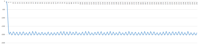
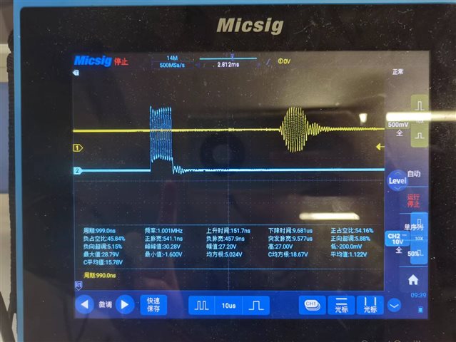
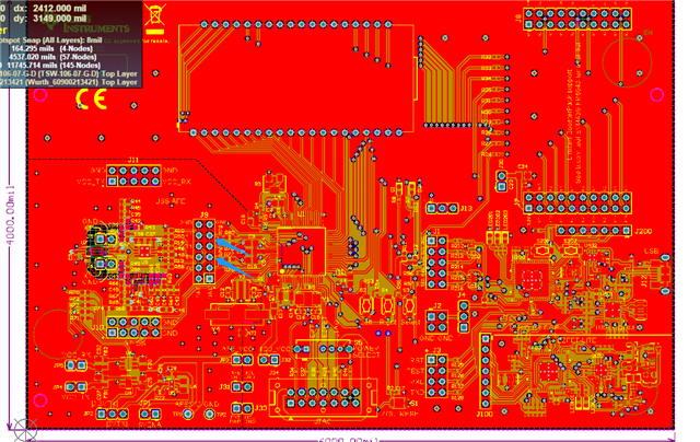
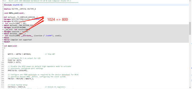
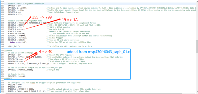
Our company plan to design a water meter using msp430fr6043. We have modified the capacitances and resistances on the EVM430-FR6043 in Figure 1. We used the code examples for msp430fr6043 which named msp430fr6043_saph_01.c, and the code is then posted. We used an oscilloscope to view the waveform of the CH0_OUT pin, as shown in Figure 2,3. The problem we faced was that the oscilloscope waveform was not a square wave, and we suspected that it was not an excitation signal. We want to generate an incentive signal first, but we do not know what is wrong with this, please inform us, thank you very much!
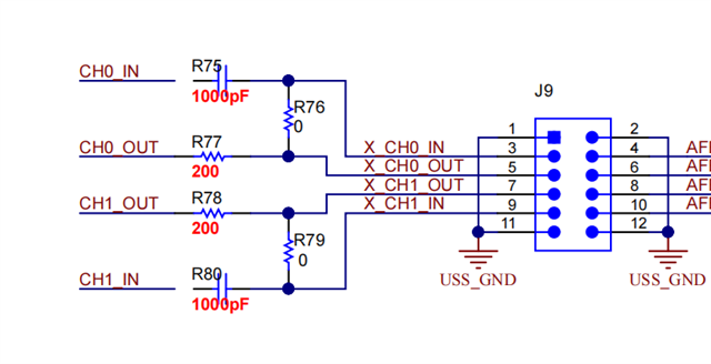
Figure 1
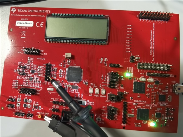
Figure 2
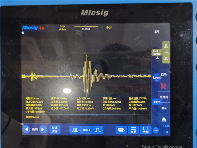
Figure 3
msp430fr6043_saph_01.c
#include <msp430.h>
#define OSCTYPE__CRYSTAL OSCTYPE_0
void HSPLL_init(void);
int main(void)
{
WDTCTL = WDTPW | WDTHOLD; // Stop WDT
// Configure P1.5 as output for LED
P1OUT &= ~BIT5;
P1DIR |= BIT5;
// Disable the GPIO power-on default high-impedance mode to activate
// previously configured port settings
PM5CTL0 &= ~LOCKLPM5;
// Clock System Setup
CSCTL0_H = CSKEY_H; // Unlock CS registers
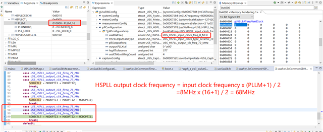
CSCTL1 = DCOFSEL_3 | DCORSEL; // Set DCO to 8MHz
// Set SMCLK = MCLK = DCO, ACLK = VLOCLK
CSCTL2 = SELA__VLOCLK | SELS__DCOCLK | SELM__DCOCLK;
CSCTL3 = DIVA__1 | DIVS__8 | DIVM__8; // MCLK = SMCLK = 1MHz
CSCTL0_H = 0; // Lock CS registers
HSPLL_init(); // Initialize the HSPLL and wait for it to lock
// Set up the PPG settings
SAPHKEY = KEY; // Unlock the SAPH registers
SAPHPGC = PLEV_0 | PPOL_0 | 0x000A; // 10 excitation pulses, 0 stop pulses, output low when inactive, high polarity
SAPHPGLPER = 40; // Low phase = 40 HSPLL cycles = 500ns
SAPHPGHPER = 40; // High phase = 40 HSPLL cycles = 500ns
SAPHPGCTL = TRSEL_2 | PPGCHSEL_0 | PGSEL_0; // TA2.1 trigger, CH0 output, register mode
// Set up the PHY to output PPG on dedicated CH0_OUT pin
SAPHOSEL = PCH0SEL__PPGSE; // Output PPG
// Enable the PPG
SAPHPGCTL |= PPGEN;
// Configure TA2.1 for ~1/sec to trigger the pulse generation and toggle LED
TA2CCR0 = 9400;
TA2CCR1 = 4700;
TA2CCTL1 = OUTMOD_7 | CCIE; // Enable output signal to trigger PPG, enable Interrupt
TA2CTL = TASSEL__ACLK | TACLR | MC__UP; // Timer sourced from ACLK (VLO), clear timer
while(1)
{
__bis_SR_register(LPM0_bits | GIE); // Enter LPM3 w/interrupt
__no_operation(); // For debug
}
}
// Timer A2 interrupt service routine
#if defined(__TI_COMPILER_VERSION__) || defined(__IAR_SYSTEMS_ICC__)
#pragma vector = TIMER2_A1_VECTOR
__interrupt void Timer2_A1_ISR(void)
#elif defined(__GNUC__)
void __attribute__ ((interrupt(TIMER2_A1_VECTOR))) Timer2_A1_ISR (void)
#else
#error Compiler not supported!
#endif
{
switch(__even_in_range(TA2IV, TAIV__TAIFG))
{
case TAIV__NONE: break; // No interrupt
case TAIV__TACCR1:
P1OUT ^= BIT5; // Toggle LED to show new cycle
break;
case TAIV__TAIFG: break; // overflow
default: break;
}
}
void HSPLL_init(void)
{
// Configure USSXT Oscillator
HSPLLUSSXTLCTL = OSCTYPE__CRYSTAL | USSXTEN;
// Set up timer to wait in LPM for crystal stabilization time = 4096 clocks for crystal resonator.
// For 8MHz XTAL, 4096 clocks = 512us. Using VLO = 9.4kHz, wait 5 timer clock cycles = 532us.
TA4CCR0 = 5;
TA4CCTL0 = CCIE; // Enable Interrupt
TA4CTL = TASSEL__ACLK | TACLR | MC__UP; // Timer sourced from ACLK (VLO), clear timer
__bis_SR_register(LPM3_bits | GIE); // Enter LPM3 w/interrupt
__no_operation(); // For debug
// Check if oscillator is stable
while((HSPLLUSSXTLCTL & OSCSTATE) == 0);
// Output oscillator on pin
HSPLLUSSXTLCTL &= ~XTOUTOFF;
// Init PLL
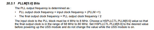
// Use the PLLM setting to get 80MHz output from our 8MHz input
// Equation: PLL output clock frequency x 2 = input clock frequency x (PLLM+1)
// Input clock frequency = 8MHz
// Desired PLL output clock frequency = 80MHz
// PLLM = 19
HSPLLCTL = PLLM4 | PLLM1 | PLLM0 | PLLINFREQ; //PLLM = 19, PLL input frequency > 6MHz
// Power up the UUPS to start the PLL
UUPSCTL |= USSPWRUP;
// Wait for UUPS to power up
while((UUPSCTL & UPSTATE_3) != UPSTATE_3);
// Wait for PLL to lock
while(!(HSPLLCTL & PLL_LOCK));
}
// Timer A4 interrupt service routine
#if defined(__TI_COMPILER_VERSION__) || defined(__IAR_SYSTEMS_ICC__)
#pragma vector = TIMER4_A0_VECTOR
__interrupt void Timer4_A0_ISR(void)
#elif defined(__GNUC__)
void __attribute__ ((interrupt(TIMER4_A0_VECTOR))) Timer4_A0_ISR (void)
#else
#error Compiler not supported!
#endif
{
// Stop the timer and wake from LPM
TA4CTL = MC__STOP;
__bic_SR_register_on_exit(LPM3_bits | GIE);
__no_operation();
}