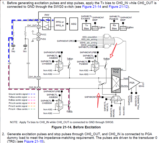
Other Parts Discussed in Thread: MSP430FR6041, , MSP430FR5043, MSP430FR5041, EVM430-FR6043
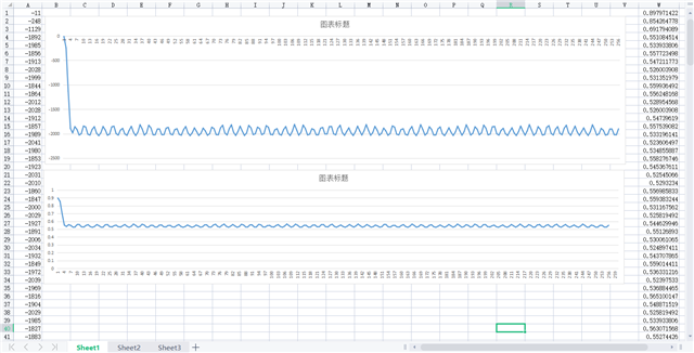
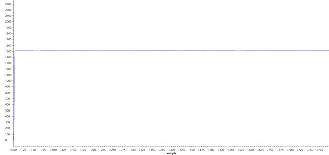
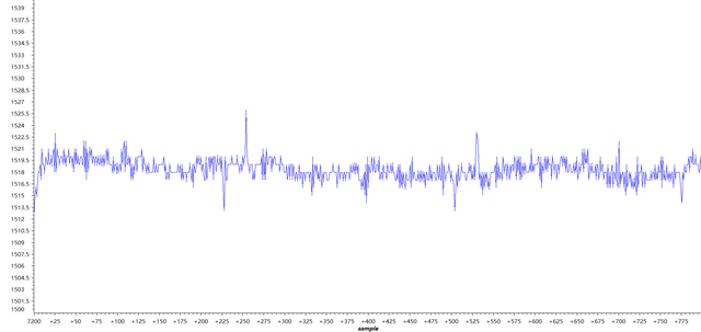
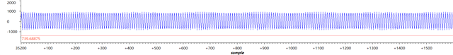
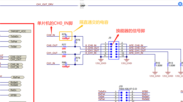
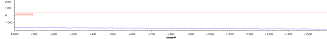
您好,我们使用了“MSP430FR6043_MSP430FR6041_MSP430FR5043_MSP430FR5041_Code_Examples”里的“msp430fr6043_saph_01.c”和“msp430fr6043_sdhs_01.c”例程,用示波器可以看到换能器接收到由另一个换能器发送的激励波形,但是程序里的results数组观察不到有效的波形,形状差不多如图1所示,请问怎样才能观察到正确的波形呢?
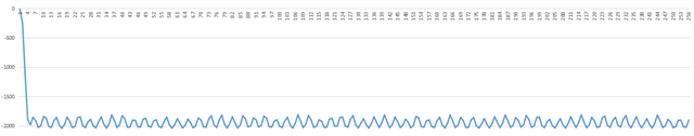
图1
/* --COPYRIGHT--,BSD_EX
* Copyright (c) 2017, Texas Instruments Incorporated
* All rights reserved.
*
* Redistribution and use in source and binary forms, with or without
* modification, are permitted provided that the following conditions
* are met:
*
* * Redistributions of source code must retain the above copyright
* notice, this list of conditions and the following disclaimer.
*
* * Redistributions in binary form must reproduce the above copyright
* notice, this list of conditions and the following disclaimer in the
* documentation and/or other materials provided with the distribution.
*
* * Neither the name of Texas Instruments Incorporated nor the names of
* its contributors may be used to endorse or promote products derived
* from this software without specific prior written permission.
*
* THIS SOFTWARE IS PROVIDED BY THE COPYRIGHT HOLDERS AND CONTRIBUTORS "AS IS"
* AND ANY EXPRESS OR IMPLIED WARRANTIES, INCLUDING, BUT NOT LIMITED TO,
* THE IMPLIED WARRANTIES OF MERCHANTABILITY AND FITNESS FOR A PARTICULAR
* PURPOSE ARE DISCLAIMED. IN NO EVENT SHALL THE COPYRIGHT OWNER OR
* CONTRIBUTORS BE LIABLE FOR ANY DIRECT, INDIRECT, INCIDENTAL, SPECIAL,
* EXEMPLARY, OR CONSEQUENTIAL DAMAGES (INCLUDING, BUT NOT LIMITED TO,
* PROCUREMENT OF SUBSTITUTE GOODS OR SERVICES; LOSS OF USE, DATA, OR PROFITS;
* OR BUSINESS INTERRUPTION) HOWEVER CAUSED AND ON ANY THEORY OF LIABILITY,
* WHETHER IN CONTRACT, STRICT LIABILITY, OR TORT (INCLUDING NEGLIGENCE OR
* OTHERWISE) ARISING IN ANY WAY OUT OF THE USE OF THIS SOFTWARE,
* EVEN IF ADVISED OF THE POSSIBILITY OF SUCH DAMAGE.
*
*******************************************************************************
*
* MSP430 CODE EXAMPLE DISCLAIMER
*
* MSP430 code examples are self-contained low-level programs that typically
* demonstrate a single peripheral function or device feature in a highly
* concise manner. For this the code may rely on the device's power-on default
* register values and settings such as the clock configuration and care must
* be taken when combining code from several examples to avoid potential side
* effects. Also see www.ti.com/grace for a GUI- and www.ti.com/msp430ware
* for an API functional library-approach to peripheral configuration.
*
* --/COPYRIGHT--*/
//******************************************************************************
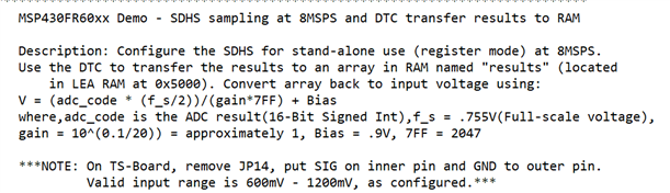
// MSP430FR60xx Demo - SDHS sampling at 8MSPS and DTC transfer results to RAM
//
// Description: Configure the SDHS for stand-alone use (register mode) at 8MSPS.
// Use the DTC to transfer the results to an array in RAM named "results" (located
// in LEA RAM at 0x5000). Convert array back to input voltage using:
// V = (adc_code * (f_s/2))/(gain*7FF) + Bias
// where,adc_code is the ADC result(16-Bit Signed Int),f_s = .755V(Full-scale voltage),
// gain = 10^(0.1/20)) = approximately 1, Bias = .9V, 7FF = 2047
//
// ***NOTE: On TS-Board, remove JP14, put SIG on inner pin and GND to outer pin.
// Valid input range is 600mV - 1200mV, as configured.***
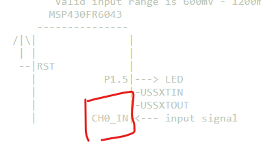
// MSP430FR6043
// ---------------
// /|\| |
// | | |
// --|RST |
// | P1.5|---> LED
// | |-USSXTIN
// | |-USSXTOUT
// | CH0_IN|<--- input signal
//
// Gary Gao & Matt Calvo
// Texas Instruments Inc.
// February 2018
// Built with IAR Embedded Workbench V7.10 & Code Composer Studio V7.3
//******************************************************************************
#include <msp430.h>
#define OSCTYPE__CRYSTAL OSCTYPE_0
void HSPLL_init(void);
#if defined(__TI_COMPILER_VERSION__)
#pragma DATA_SECTION(results, ".leaRAM")
#pragma RETAIN(results)
int results[1800] = {0};
#elif defined(__IAR_SYSTEMS_ICC__)
#pragma location=0x5000
__no_init int results[1024];
#pragma required = results
#elif defined(__GNUC__)
int results[1800] __attribute__ ((section (".leaRAM"), used));
#else
#error Compiler not supported!
#endif
int main(void)
{
WDTCTL = WDTPW | WDTHOLD; // Stop WDT
// Configure P1.5 as output for LED
P1OUT &= ~BIT5;
P1DIR |= BIT5;
// Disable the GPIO power-on default high-impedance mode to activate
// previously configured port settings
PM5CTL0 &= ~LOCKLPM5;
// Configure one FRAM waitstate as required by the device datasheet for MCLK
// operation beyond 8MHz _before_ configuring the clock system.
FRCTL0 = FRCTLPW | NWAITS_1;
// Clock System Setup
CSCTL0_H = CSKEY_H; // Unlock CS registers
// Per Device Errata(CS12) set divider to 4 before changing frequency to
// prevent out of spec operation from overshoot transient
CSCTL3 = DIVA__4 | DIVS__4 | DIVM__4; // Set all corresponding clk sources to divide by 4 for errata(CS12)
CSCTL1 = DCOFSEL_4 | DCORSEL; // Set DCO to 16MHz
// Delay by ~10us to let DCO settle. 60 cycles = 20 cycles buffer + (10us / (1/4MHz))
__delay_cycles(60);
CSCTL3 = DIVA__1 | DIVS__1 | DIVM__1; // Set all dividers to 1 for 16MHz operation
CSCTL3 = DIVA__1 | DIVS__1 | DIVM__1; // MCLK = SMCLK = 16MHz
CSCTL0_H = 0; // Lock CS registers
//Setup SAPH Bias Register Controlled
SAPHKEY = KEY;
SAPHBCTL &= ~ASQBSC; //Tx bias and Rx bias switches control source select; 0h (R/W) = Bias switches are controlled by SAPHBCTL.CH0EBSW, SAPHBCTL.CH1EBSW, SAPHBCTL.PGABSW bits (register mode)
SAPHBCTL |= CPDA; //Enable the power supply (Charge Pump) for the the input multiplexer during data acquisition. 1h (R/W) = Keep turning on the charge pump during data acquisition.
SAPHICTL0 = 0; //Input Multiplexer Channel Select
SAPHKEY = KEY+1;
//Setup the SDHS with register mode
SDHSCTL0 = TRGSRC_0 | AUTOSSDIS_1 | DFMSEL_0;// Software trigger,Left, 2s complement format
SDHSCTL1 = OSR_4; // OSR = 10 (80MHz/10 = 8MSPS). CS must set MCLK >= 8MHz.
SDHSCTL2 = 1799; // SMPSZ = 255+1 samples
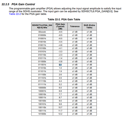
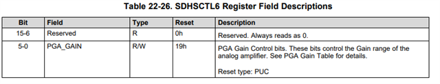
SDHSCTL6 = 0x20; // PGA Gain 0.1 dB
SDHSCTL7 = 0xC; // MODOPTI = 0xC (80MHz PLL output frequency)
SDHSDTCDA = 0x800; // DTC transfer data to start of LEA RAM
SDHSIMSC = ACQDONE; // Enable acquisition done interrupt (after 256 samples transferred)
SDHSCTL3 = TRIGEN_1; // Enable trigger
SDHSCTL4 = SDHSON; // Turn on SD and start conversion
__delay_cycles(640); // Delay for PGA worst case 40us settling time
HSPLL_init(); // Initialize the HSPLL and wait for it to lock
///*SAPH
// Set up the PPG settings
SAPHKEY = KEY; // Unlock the SAPH registers
SAPHPGC = PLEV_0 | PPOL_0 | 0x000A; // 10 excitation pulses, 0 stop pulses, output low when inactive, high polarity
SAPHPGLPER = 40; // Low phase = 40 HSPLL cycles = 500ns
SAPHPGHPER = 40; // High phase = 40 HSPLL cycles = 500ns
SAPHPGCTL = TRSEL_2 | PPGCHSEL_0 | PGSEL_0; // TA2.1 trigger, CH0 output, register mode
// Set up the PHY to output PPG on dedicated CH0_OUT pin
SAPHOSEL = PCH0SEL__PPGSE; // Output PPG
// Enable the PPG
SAPHPGCTL |= PPGEN;
//SAPH*/
// Configure TA2.1 for 1/sec to trigger the pulse generation and toggle LED
TA2CCR0 = 9400;
TA2CCR1 = 4700;
TA2CCTL1 = OUTMOD_7 | CCIE; // Enable output signal to trigger PPG, enable Interrupt
TA2CTL = TASSEL__ACLK | TACLR | MC__UP; // Timer sourced from ACLK (VLO), clear timer
while(1)
{
__bis_SR_register(LPM0_bits | GIE); // Enter LPM0 w/interrupt
__no_operation(); // For debug
}
}
// Timer A2 interrupt service routine
#if defined(__TI_COMPILER_VERSION__) || defined(__IAR_SYSTEMS_ICC__)
#pragma vector = TIMER2_A1_VECTOR
__interrupt void Timer2_A1_ISR(void)
#elif defined(__GNUC__)
void __attribute__ ((interrupt(TIMER2_A1_VECTOR))) Timer2_A1_ISR (void)
#else
#error Compiler not supported!
#endif
{
switch(__even_in_range(TA2IV, TAIV__TAIFG))
{
case TAIV__NONE: break; // No interrupt
case TAIV__TACCR1:
SDHSCTL4&= ~SDHSON;
SDHSCTL5 &= ~SSTART;
SDHSCTL3 = 0;
SDHSDTCDA = 0x800;
SDHSCTL3 = TRIGEN_1;
SDHSCTL4 = SDHSON;
SDHSCTL5 |= SSTART; // Start conversion
__no_operation();
break;
case TAIV__TAIFG: // overflow
__no_operation();
break;
default: break;
}
}
// SDHS interrupt service routine
#if defined(__TI_COMPILER_VERSION__) || defined(__IAR_SYSTEMS_ICC__)
#pragma vector = SDHS_VECTOR
__interrupt void SDHS_ISR(void)
#elif defined(__GNUC__)
void __attribute__ ((interrupt(SDHS_VECTOR))) SDHS_ISR (void)
#else
#error Compiler not supported!
#endif
{
switch(__even_in_range(SDHSIIDX, IIDX_6))
{
case IIDX_0: break; // No interrupt
case IIDX_1:
__no_operation();
break; // OVF interrupt
case IIDX_2: // ACQDONE interrupt
P1OUT ^= BIT5; // Toggle LED to show new cyclelll
__delay_cycles(1000);
__no_operation(); // Put breakpoint here to view results
break;
case IIDX_3: break; // SSTRG interrupt
case IIDX_4: break; // DTRDY interrupt
case IIDX_5: break; // WINHI interrupt
case IIDX_6: break; // WINLO interrupt
default: break;
}
}
void HSPLL_init(void)
{
// Configure USSXT Oscillator
HSPLLUSSXTLCTL = OSCTYPE__CRYSTAL | USSXTEN;
// Set up timer to wait in LPM for crystal stabilization time = 4096 clocks for crystal resonator.
// For 8MHz XTAL, 4096 clocks = 512us. Using VLO = 9.4kHz, wait 5 timer clock cycles = 532us.
TA4CCR0 = 5;
TA4CCTL0 = CCIE; // Enable Interrupt
TA4CTL = TASSEL__ACLK | TACLR | MC__UP; // Timer sourced from ACLK (VLO), clear timer
__bis_SR_register(LPM3_bits | GIE); // Enter LPM3 w/interrupt
__no_operation(); // For debug
// Check if oscillator is stable
while((HSPLLUSSXTLCTL & OSCSTATE) == 0);
// Output oscillator on pin
HSPLLUSSXTLCTL &= ~XTOUTOFF;
// Init PLL
// Use the PLLM setting to get 80MHz output from our 8MHz input
// Equation: PLL output clock frequency x 2 = input clock frequency x (PLLM+1)
// Input clock frequency = 8MHz
// Desired PLL output clock frequency = 80MHz
// PLLM = 19
HSPLLCTL = PLLM4 | PLLM1 | PLLM0 | PLLINFREQ; //PLLM = 19, PLL input frequency > 6MHz
// Power up the UUPS to start the PLL
UUPSCTL |= USSPWRUP;
// Wait for UUPS to power up
while((UUPSCTL & UPSTATE_3) != UPSTATE_3);
// Wait for PLL to lock
while(!(HSPLLCTL & PLL_LOCK));
}
// Timer A4 interrupt service routine
#if defined(__TI_COMPILER_VERSION__) || defined(__IAR_SYSTEMS_ICC__)
#pragma vector = TIMER4_A0_VECTOR
__interrupt void Timer4_A0_ISR(void)
#elif defined(__GNUC__)
void __attribute__ ((interrupt(TIMER4_A0_VECTOR))) Timer4_A0_ISR (void)
#else
#error Compiler not supported!
#endif
{
// Stop the timer and wake from LPM
TA4CTL = MC__STOP;
__bic_SR_register_on_exit(LPM3_bits | GIE);
__no_operation();
}