

错误信息:
C28xx: File Loader: Data verification failed at address 0x00210000 Please verify target memory and memory map. C28xx: GEL: File: D:\workspace\SXD28335B\SXD28335B_STU_examples\Example_2833x_ECanBack2Back\Debug\Example_2833xECanBack2Back.out: a data verification error occurred, file load failed.
除了28335_RAM_lnk.cmd文件中增加了zone7C 和zone6 并将.ebss指向zone6,.txt指向zone7c外没做其他更改
MEMORY
{
PAGE 0 :
/* BEGIN is used for the "boot to SARAM" bootloader mode */
BEGIN : origin = 0x000000, length = 0x000002 /* Boot to M0 will go here */
RAMM0 : origin = 0x000050, length = 0x0003B0
RAML0 : origin = 0x008000, length = 0x001000
RAML1 : origin = 0x009000, length = 0x001000
RAML2 : origin = 0x00A000, length = 0x001000
RAML3 : origin = 0x00B000, length = 0x001000
ZONE7A : origin = 0x200000, length = 0x00FC00 /* XINTF zone 7 - program space */
CSM_RSVD : origin = 0x33FF80, length = 0x000076 /* Part of FLASHA. Program with all 0x0000 when CSM is in use. */
CSM_PWL : origin = 0x33FFF8, length = 0x000008 /* Part of FLASHA. CSM password locations in FLASHA */
ADC_CAL : origin = 0x380080, length = 0x000009
RESET : origin = 0x3FFFC0, length = 0x000002
IQTABLES : origin = 0x3FE000, length = 0x000b50
IQTABLES2 : origin = 0x3FEB50, length = 0x00008c
FPUTABLES : origin = 0x3FEBDC, length = 0x0006A0
BOOTROM : origin = 0x3FF27C, length = 0x000D44
/*zhijie add*/
ZONE0 : origin = 0x004000, length = 0x001000
ZONE7C : origin = 0x210000, length = 0x003000
PAGE 1 :
/* BOOT_RSVD is used by the boot ROM for stack. */
/* This section is only reserved to keep the BOOT ROM from */
/* corrupting this area during the debug process */
BOOT_RSVD : origin = 0x000002, length = 0x00004E /* Part of M0, BOOT rom will use this for stack */
RAMM1 : origin = 0x000400, length = 0x000400 /* on-chip RAM block M1 */
RAML4 : origin = 0x00C000, length = 0x001000
RAML5 : origin = 0x00D000, length = 0x001000
RAML6 : origin = 0x00E000, length = 0x001000
RAML7 : origin = 0x00F000, length = 0x001000
ZONE7B : origin = 0x20FC00, length = 0x000400 /* XINTF zone 7 - data space */
ZONE6 : origin = 0x100000, length = 0x040000
}
SECTIONS
{
/* Setup for "boot to SARAM" mode:
The codestart section (found in DSP28_CodeStartBranch.asm)
re-directs execution to the start of user code. */
codestart : > BEGIN, PAGE = 0
ramfuncs : > RAML0, PAGE = 0
/*.text : > RAML1, PAGE = 0*/
.text : > ZONE7C, PAGE = 0
.cinit : > RAML0, PAGE = 0
.pinit : > RAML0, PAGE = 0
.switch : > RAML0, PAGE = 0
.stack : > RAMM1, PAGE = 1
/*.ebss : > RAML4, PAGE = 1*/
.ebss : > ZONE6, PAGE = 1
.econst : > RAML5, PAGE = 1
.esysmem : > RAMM1, PAGE = 1
IQmath : > RAML1, PAGE = 0
IQmathTables : > IQTABLES, PAGE = 0, TYPE = NOLOAD
/* Uncomment the section below if calling the IQNexp() or IQexp()
functions from the IQMath.lib library in order to utilize the
relevant IQ Math table in Boot ROM (This saves space and Boot ROM
is 1 wait-state). If this section is not uncommented, IQmathTables2
will be loaded into other memory (SARAM, Flash, etc.) and will take
up space, but 0 wait-state is possible.
*/
/*
IQmathTables2 : > IQTABLES2, PAGE = 0, TYPE = NOLOAD
{
IQmath.lib<IQNexpTable.obj> (IQmathTablesRam)
}
*/
FPUmathTables : > FPUTABLES, PAGE = 0, TYPE = NOLOAD
DMARAML4 : > RAML4, PAGE = 1
DMARAML5 : > RAML5, PAGE = 1
DMARAML6 : > RAML6, PAGE = 1
DMARAML7 : > RAML7, PAGE = 1
ZONE7DATA : > ZONE7B, PAGE = 1
.reset : > RESET, PAGE = 0, TYPE = DSECT /* not used */
csm_rsvd : > CSM_RSVD PAGE = 0, TYPE = DSECT /* not used for SARAM examples */
csmpasswds : > CSM_PWL PAGE = 0, TYPE = DSECT /* not used for SARAM examples */
/* Allocate ADC_cal function (pre-programmed by factory into TI reserved memory) */
.adc_cal : load = ADC_CAL, PAGE = 0, TYPE = NOLOAD
}
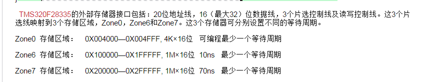
TMS320F28335的外部存储器接口包括:20位地址线,16(最大32)位数据线,3个片选控制线及读写控制线。这3个片选线映射到3个存储区域,Zone0,Zone6和Zone7。这3个存储器可分别设置不同的等待周期。
Zone0 存储区域: 0X004000—0X004FFF, 4K×16位 可编程最少一个等待周期
Zone6 存储区域: 0X100000—0X1FFFFF, 1M×16位 10ns 最少一个等待周期
Zone7 存储区域: 0X200000—0X2FFFFF, 1M×16位 70ns 最少一个等待周期
我觉得我的内存划分没有问题啊

