This thread has been locked.

If you have a related question, please click the "Ask a related question" button in the top right corner. The newly created question will be automatically linked to this question.

关于INA219的配置和数据获取的问题

Other Parts Discussed in Thread: INA219

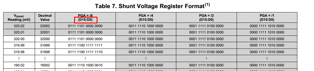
最近在看INA219的芯片资料,看得云里雾里。请各位大神解答。首先关于内部ADC的配置,里面涉及到了两个ADC,BADC和SADC,总线ADC和分流电阻ADC,datasheet给出信息,可以配置最高分辨率为12位。但是Table7 中为什么显示了16位的数据?

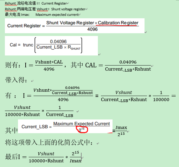
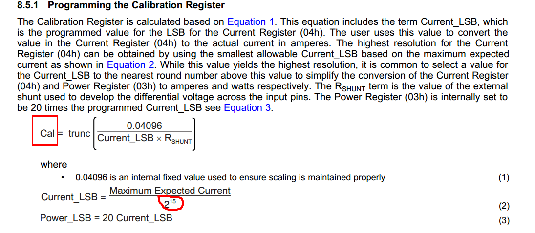
其次,程序配置校准寄存器那里为什么要取一个接近的值作为Current_LSB?完全看不懂校准寄存器的原理及作用。

  • 您好 ,12bit是ADC的分辨率,而Table 7的15bit是分压电阻Rshunt的电压Vshunt用16bit 二进制来表示。因为寄存器是16bit的。
  • Vshunt是直接由芯片内部ADC测量后存在shunt voltage register中的吗?如果是这样的话,它是怎么做到存储的最小电压LSB小于ADC的分辨率的?比如在Rshunt上形成的电压为320mV,那么ADC为12bits,可操作的最小量LSB=320/2^12 = 78.1uV,但是shunt voltage register中的LSB为10uV。远小于ADC的LSB,这是怎么回事?
  • 我通过芯片手册上的公式,化简了一下电流计算公式,化简过程如下:

    第一项Vshunt/(100000*Rshunt)就是测量的电流值,单位为A。那么后面一项的校准参数,但是看不懂校准参数的作用是什么,因为Imax这个值是自己设定写入寄存器的,Imax的值将改变获取的电流值,那我怎么评估电流精度是不是ok的呢?

  • 您好,您可以参考下datasheet page20中8.6.3.1 Shunt Voltage Register 部分的介绍,介绍了如何将Vshunt电压转换成2进制存储到shunt voltage register中的。 举例比如Vshunt=320mV,
    For a value of VSHUNT = –320 mV:
    1. Taketheabsolutevalue(includeaccuracyto0.01mV)→320.00 2. Translatethisnumbertoawholedecimalnumber→32000
    3. Convert it to binary → 111 1101 0000 0000
    4. Complement the binary result : 000 0010 1111 1111
    5. Add1totheComplementtocreatetheTwo’sComplementformattedresult→000001100000000
    6. Extend the sign and create the 16-bit word: 1000 0011 0000 0000 = 8300h (Remember to extend the sign to all sign-bits, as necessary based on the PGA setting.)