Hi support!
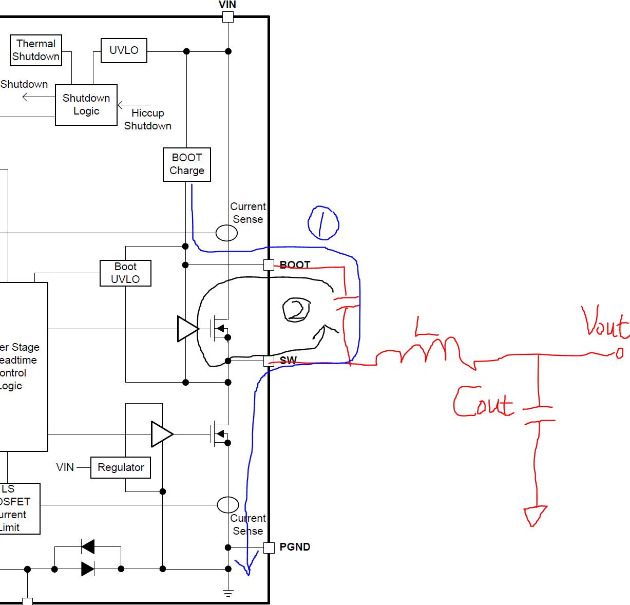
关于TPS562200 VBST管脚与SW管脚之间的电容的作用,敬请指教。因为有一个项目中,用了TPS562200,这个电容的一端接在VBST管脚,另一端却接在了电感的后端,导致输出功率问题,请问,这个电容的作用?以及为什么一定要放在电感的前端?谢谢!
Hi support!
关于TPS562200 VBST管脚与SW管脚之间的电容的作用,敬请指教。因为有一个项目中,用了TPS562200,这个电容的一端接在VBST管脚,另一端却接在了电感的后端,导致输出功率问题,请问,这个电容的作用?以及为什么一定要放在电感的前端?谢谢!