

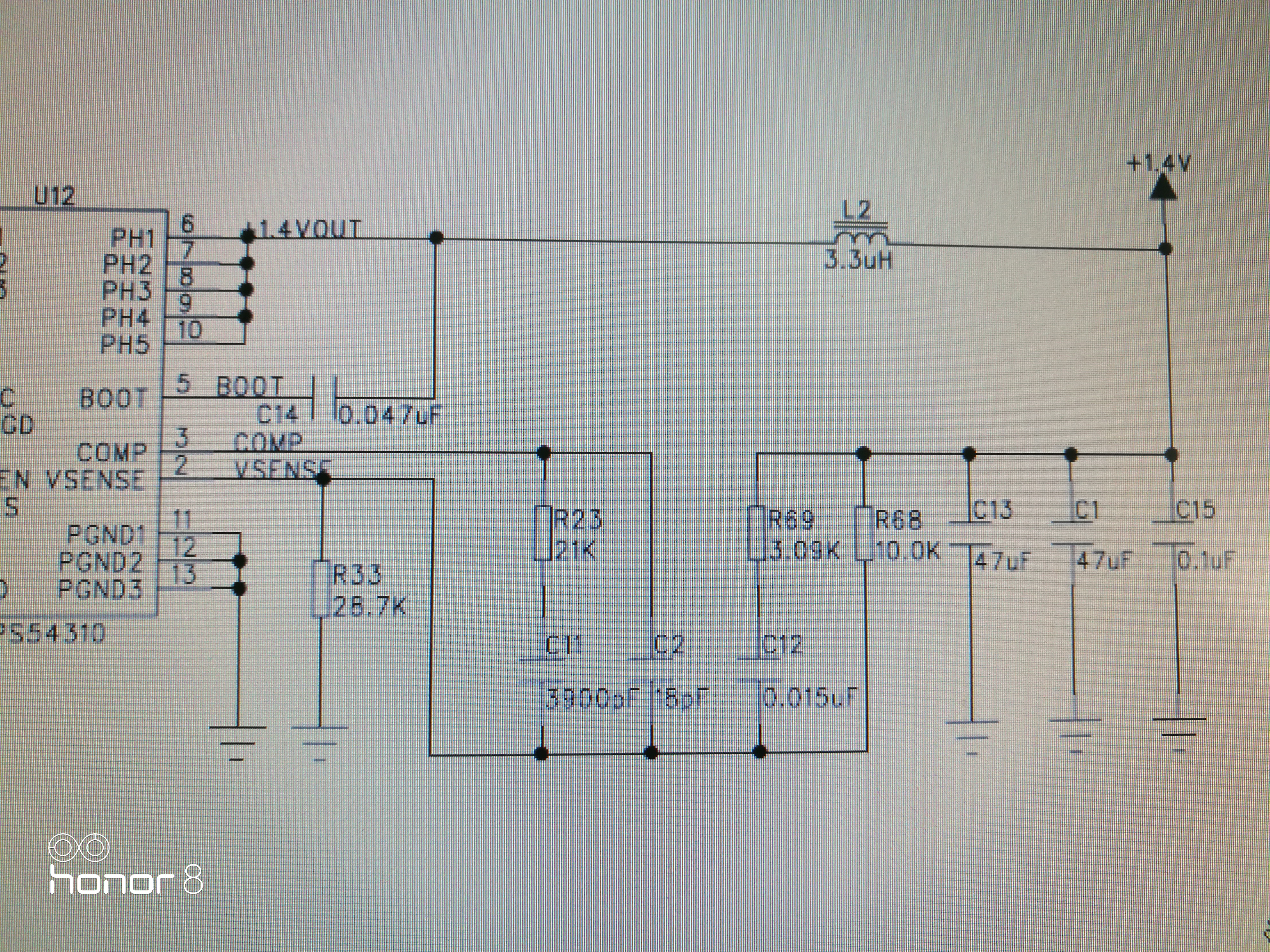
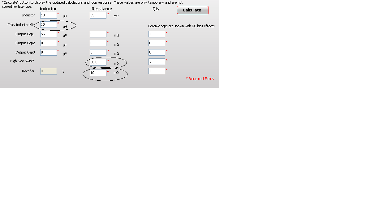
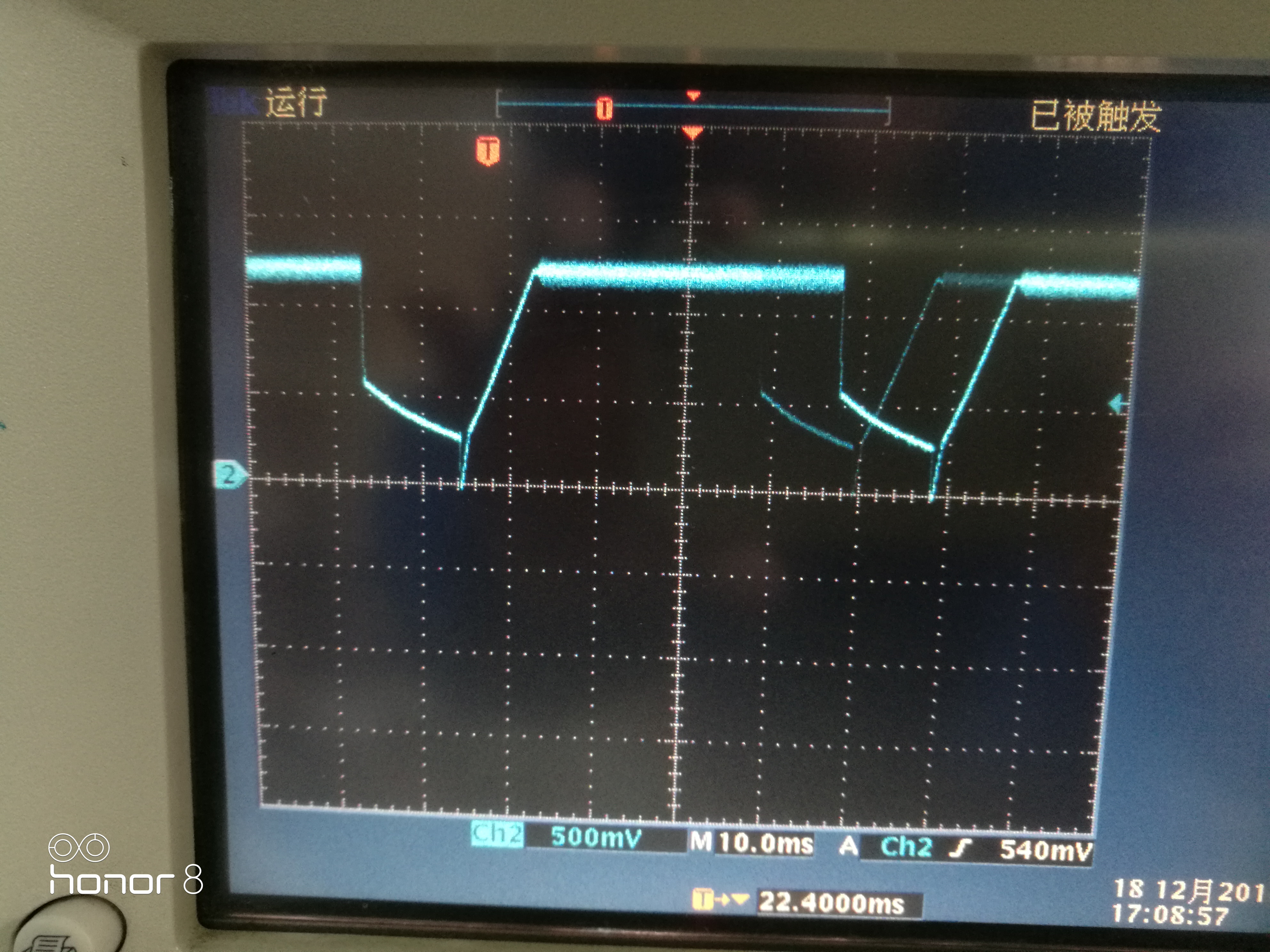
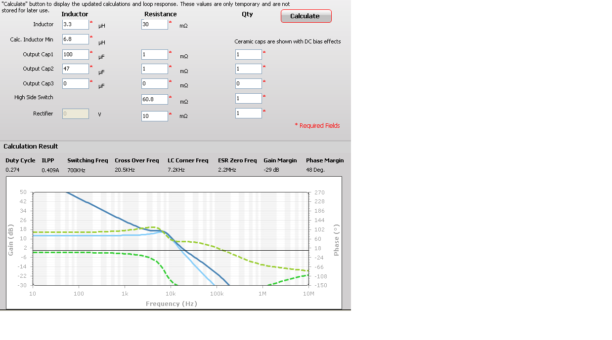
项目中使用TPS54310芯片将系统输入电压5.5V左右转换为1.2V供TMS320C6416系列DSP内核电压,通过监测5.5V稳定,但芯片TPS54310输出1.2V偶尔会出现从1.2V掉到0V的情况,持续20ms左右又会迅速拉升到1.2V,导致DSP无法正常运行,,,请教下各位,此种情况我们应该从哪些方面定位故障原因,谢谢
项目中使用TPS54310芯片将系统输入电压5.5V左右转换为1.2V供TMS320C6416系列DSP内核电压,通过监测5.5V稳定,但芯片TPS54310输出1.2V偶尔会出现从1.2V掉到0V的情况,持续20ms左右又会迅速拉升到1.2V,导致DSP无法正常运行,,,请教下各位,此种情况我们应该从哪些方面定位故障原因,谢谢

