This thread has been locked.

If you have a related question, please click the "Ask a related question" button in the top right corner. The newly created question will be automatically linked to this question.

F28379D双核程序调试问题

Other Parts Discussed in Thread: CONTROLSUITE

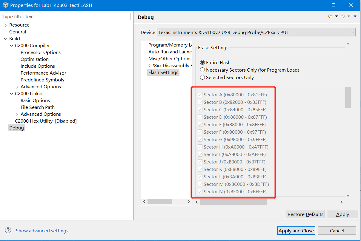
在使用controlsuit里面的controlSUITE\device_support\F2837xD\v210\F2837xD_examples_Dual\blinky_dc文件夹里面的例程,把CPU1和CPU2都导入了,build后选定CPU1的那个工程,点击Debug,然后在下面弹窗时全都勾选上了,烧录... ...

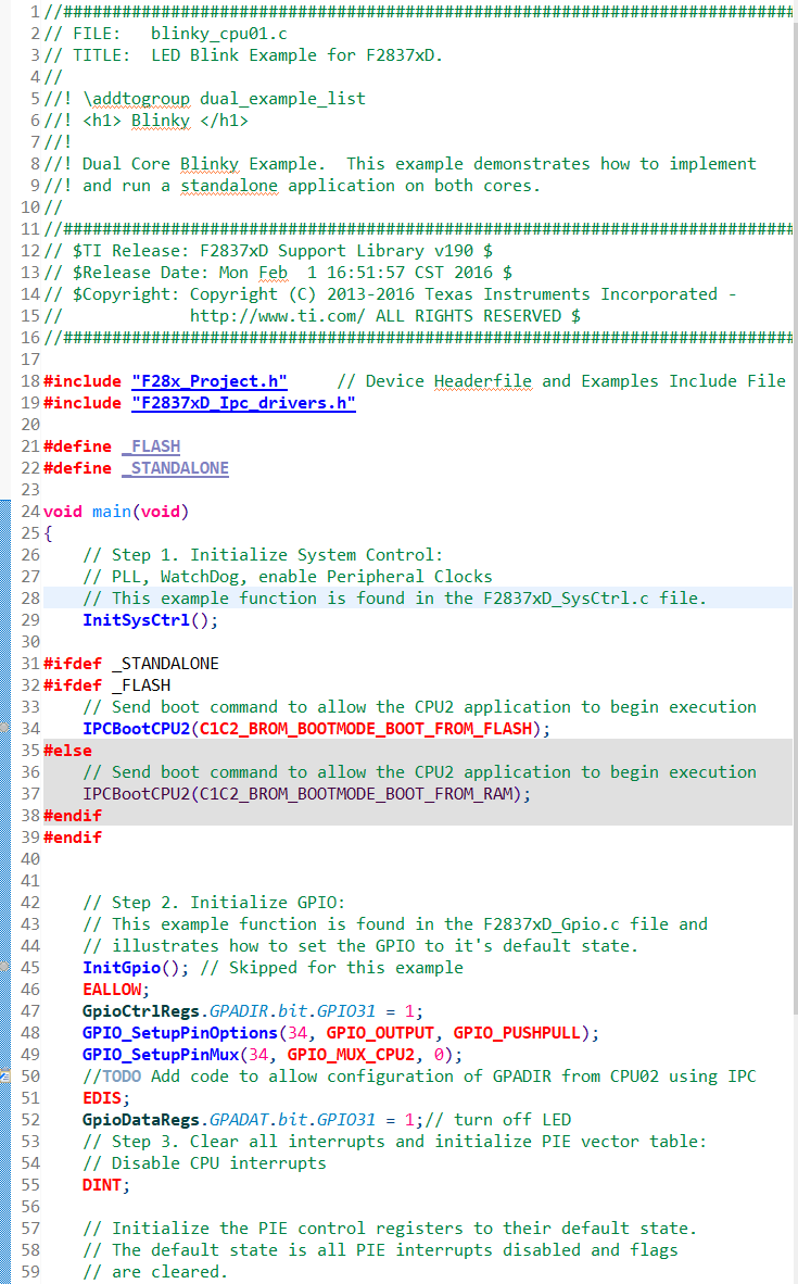
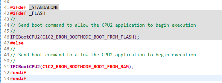
在cpu1那个程序中,我为了让CPU1来控制启动CPU2,就添加了一个宏定义,启用了IPCBootCPU2(C1C2_BROM_BOOTMODE_BOOT_FROM_RAM)这个函数

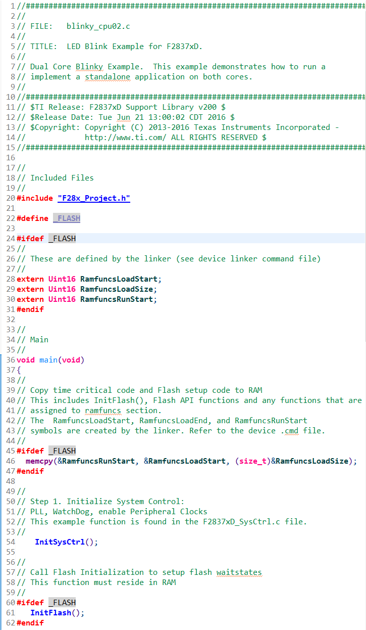
然后cpu2借鉴C28x_Microcontroller_ODW_2-0.pdf中的步骤给烧进去cpu2配套的程序了

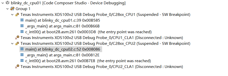
但这时选定cpu1,run起来后卡到这里了:

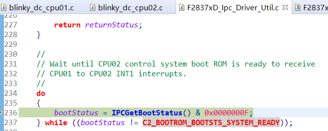
bootStatus的值为0,也就是说CPU2并没有被CPU1给控制启动了,这个为什么会卡到这里呢?到底应该如何做才能让CPU1控制启动CPU2呢,而不是采用C28x_Microcontroller_ODW_2-0.pdf里面的方式,分别启动CPU。

  • 您现在是在线调试?

    若是要debug, 烧写CPU1 FALSH DEBUG或者RAM DEBUG,CPU2烧写两个都可以,但是不能离线跑

    若是断电正常运行的话,CPU1烧写standalone,CPU2烧写FLASH
  • 我在尝试CPU2烧写FLASH,烧写方式与CPU1一样,但出现一个新的问题,CPU2的程序编译无误,可以烧写到RAM内在CPU2中正常跑通,但改烧写到FLASH时,出现以下错误,里面有一行是“No core matches the pattern 'CPU1'”,这个错误是出在什么地方呢?

    C28xx_CPU2: Error occurred during flash operation: No core matches the pattern 'CPU1'
    C28xx_CPU2: Error setting the GSxMSEL register for Flash operations
    C28xx_CPU2: Error occurred during flash operation: Timed out waiting for target to halt while executing wr_pll.alg
    C28xx_CPU2: Error writing the PLL values (Flash algorithm timed out). Operation cancelled.
    C28xx_CPU2: Perform a debugger reset and execute the Boot-ROM code (click on the RESUME button in CCS debug window) before erasing/loading the Flash. If that does not help to perform a successful Flash erase/load, check the Reset cause (RESC) register, NMI shadow flag (NMISHDFLG) register and the Boot-ROM status register for further debug.
    C28xx_CPU2: Error occurred during flash operation: No core matches the pattern 'CPU1'
    C28xx_CPU2: File Loader: Memory write failed: Unknown error
    C28xx_CPU2: GEL: File: D:\ProgramData\Workspace\Workspace_CCS_v8_0\Lab1_cpu02_testFLASH\Debug\Lab1_cpu02_testFLASH.out: Load failed.
    C28xx_CPU2: Error occurred during flash operation: No core matches the pattern 'CPU1'
    C28xx_CPU2: Error setting the GSxMSEL register for Flash operations

  • CPU2经过配置已经成功烧写FLASH了,不过无法通过CPU1控制启动CPU2,下图是我的CPU1和CPU2的程序source code:

    CPU1:

    CPU2:


    下图是我在CPU2中烧写FLASH程序时的FLASH擦除情况,请问,我这些source code和debug配置都正确么?我这样烧写是不能正常让CPU1和CPU2正常工作起来的,更别提CPU1通过IPCBootCPU2函数控制CPU2启动了。我需要怎么才能让CPU1控制启动CPU2并且两个核都能正常工作呢?下面的在往CPU2中烧写FLASH时擦除全区会不会对CPU1内的程序有影响呢?


  • 在调试的时候,不要在CPU1用IPC指令去启动CPU2.  因为CPU2在加在完程序之后,已经跳过了boot ROM里面的引导程序,直接跑到main了。

    所以已经不需要CPU1去引导了,不然就会导致CPU1一致在等待CPU2 BOOT ROM的反馈。

    IPC引导指令你在脱机跑的时候添加就可以了。

    如果你就是要在仿真的时候添加IPC引导指令,那么另外一种方式是,CPU2选择reset,然后先运行CPU2,再运行CPU1.

    Eric.

  • 感谢您的指导,我已经顺利完成双核的脱机工作了,这是我写的一篇博客记录下来了
    blog.csdn.net/.../84328254
  • 感谢您的指导,我已经顺利完成双核的脱机工作了,这是我写的一篇博客记录下来了
    blog.csdn.net/.../84328254
  • 您好,我们这边也在用28379做双核的项目,我想请教您一些问题

    在您给的博文中您比较详细的介绍了双核烧着程序的过程,不过您使用的是Ti给例程。

    我们现在两个核的工程都分别建立好了,之前都是设置的CPU1的工程。各自跑和编译都没有问题,现在走想把一个工程放到CPU2里面,里面的properies还是CPU1 RAM  和CPU1FLASH

    我们要实现工程移植到CPU2里需要修改那些内容,或者怎样修改。谢谢您!希望您能不吝赐教