If you have a related question, please click the "Ask a related question" button in the top right corner. The newly created question will be automatically linked to this question.
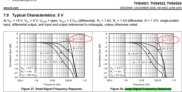
Under both large-signal output and small-signal output conditions, the bandwidth with a gain of 1 remains basically unchanged. This was obtained through the actual test?
Normalized gain plots show the small-signal frequency response (for a selected Vout) with all gain curves 'normalized' to zero dB. This removes the difficulty in reading the curve which would occur if the gain curves were plotted without being 'normalized'. For example, a 2V/V gain response would be at 6dB rather than 0dB, which would result in a positive shift of the 2V/V signal above the 1V/V signal. Normalizing the gain curves will set all gain configurations to have their flat response at 0dB, allowing for better comparison of gain peaking, roll-off, and gain flatness.
The frequency response curves are typically for a single gain configuration (such as 1V/V) with a variation of output voltages. These can be both large and small signal output voltages, or the the gain response curves can be split into separate small signal and large signal gain responses.
When you encounter a gain configuration and output voltage that is not present on the datasheet typical curves, you can either extrapolate that a larger signal at a higher gain would result in less bandwidth (for a voltage-feedback architecture device), or you can reach out to our applications team for help. We typically will not retake data unless showcasing exact data is mission critical to a business WIN or customer project.
Also, the typical characteristics curves are usually lab data taken with the device. Exceptions do occur, but these exceptions are for characteristics which are either difficult or unreliable to measure on bench.
Frequency response is rarely ever modeled and simulated, the frequency response curves for our devices come from lab data. This is true for THS4552/THS455x.
You are correct in your observation; the THS4551/2/x has a consistent G=1V/V response across small signal and large signal voltages. This will remain true, in general, as this is a low voltage FDA and cannot accept very large input signals. If this was a high voltage FDA, you would see a decrease in bandwidth if you were using a higher voltage input.
Your intuition and amplifier understanding is good; please always ask if you need help or clarification. FDAs in particular can be difficult or non-intuitive especially from a customer perspective.
Are you concerned about THS4522 and THS4552 having different measurements or methods? These are two different devices, though related, which can differ in performance between the two. The THS4552 has wider bandwidth overall, which would improve large signal bandwidth for larger output signals.
Is there a specific issue or data result we are troubleshooting here for a design? The data curves are from actual bench data for small-signal and large signal frequency response. The data on the device data sheet is correct to the device's performance.
Is your concern about replacing the THS4522 in a design with the THS4552?
If you share more I can help you find resolution. I believe I may be misunderstanding the purpose of your question, if so I apologize. Please allow me to consider your next explanation or response if I have not resolved your question.