This thread has been locked.

If you have a related question, please click the "Ask a related question" button in the top right corner. The newly created question will be automatically linked to this question.

THS7314信号问题

Other Parts Discussed in Thread: THS7314

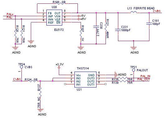
如附件电路所示,使用EL5172将差分PAL信号转换为单端PAL信号,经由THS7314芯片环路输出两路PAL信号。
调试中发现,由TP24位置输入PAL信号,经THS7314环路输出两个PAL信号给ADV7401,显示正常。
由外部输入差分PAL信号,经EL5172转换为单端PAL信号,直接输出给ADV7401,显示正常。
但是,由外部输入差分PAL信号,经EL5172转换为单端PAL信号,再经THS7314环路输出给ADV7401,则不能正常显示,图像闪烁,有时采样不到同步信号。
按照电路中EL5172配置所示,CVBS=PAL+ - PAL-.
请问THS7314与EL5172搭配存在兼容问题么? 如何解决。

  • EL5172 +-5V 供电,THS7314 3.3V 供电,要采用交流耦合,注意信号幅度,另外阻抗匹配也要加。

  • 补充一下,
    在EL5172与THS7314除了加AC couple,
    根据EL5172的datasheet,a small series resistor at the output can help
    to reduce peaking.As the load resistance
    becomes lower, the output swing is reduced respectively.

    EL5172的输出尝试+串联电阻以及减小load resistor.电阻值的选择要阻抗匹配成75ohm。另外PCB走线也要走成stip line,特征阻抗为75ohm

    而且
    The power supply pins should have a 0.1 μF to 0.01 μF capacitor placed as close as possible to these pins.
    Failure to do so may result in the THS7314 outputs ringing or have an oscillation. Additionally, a large capacitor,
    such as 22 μF to 100 μF, should be placed on the power supply line to minimize interference with 50/60 Hz line
    frequencies.

    对于EL5172也必须按下面要求做

     The power supply
    pin must be well bypassed to reduce the risk of oscillation.
    For normal single supply operation, where the VS- pin is
    connected to the ground plane, a single 4.7µF tantalum
    capacitor in parallel with a 0.1µF ceramic capacitor from VS+
    to GND will suffice. This same capacitor combination should
    be placed at each supply pin to ground if split supplies are to
    be used. In this case, the VS- pin becomes the negative
    supply rail.

  • THS7314芯片为单电源供电,不支持带负电源的CVBS信号,需要对信号做偏置处理,或者更换为正负电源供电的芯片。