Part Number: OPA860
Other Parts Discussed in Thread: OPA861
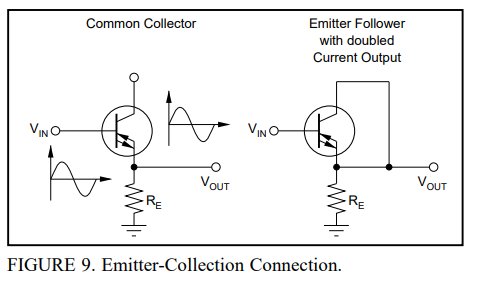
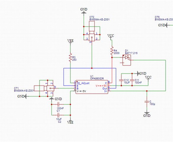
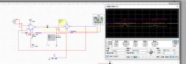
I designed a peak hold circuit using OPA860 and OPA861, a transistor amplifier chip, where the physical design and simulation design principles are similar. However, without its built-in buffer, the input and output signals are perfectly aligned to form a follower.
In the physical design, the circuit designed with OPA860 is designed according to the successful simulation circuit principle, and the output signal is still the same as the input signal to form the follower function, and the experimental result of OPA861 is the same. Thank you very much!
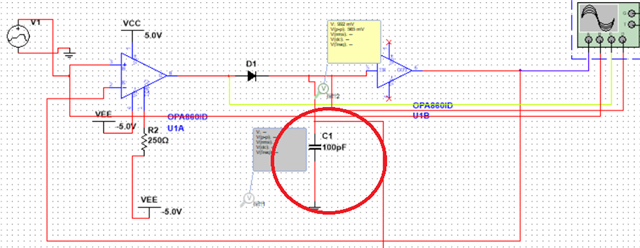
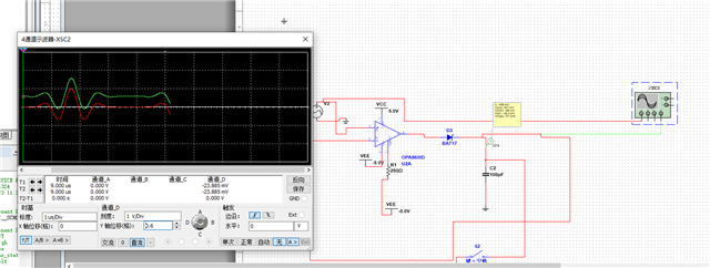
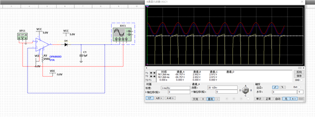
我采用了OPA860与OPA861这款跨导放大器芯片设计了一个峰值保持电路,其中实物设计与仿真设计原理类似,在仿真当中,第一个图采用了OPA860本身内置的缓冲器成功实现了峰值保持功能,然而不使用它内置缓冲器时却使得它的输入与输出信号完全一致构成了跟随器的功能。
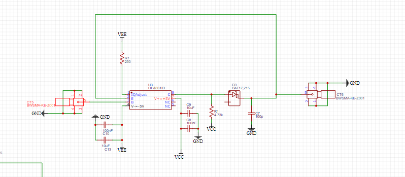
在实物设计中,采用OPA860设计的电路是按成功的仿真电路原理来设计,此时输出信号依旧跟输入信号一致构成了跟随器功能,OPA861的实验结果亦是如此,为什么会出现这种情况可以帮忙解答吗?十分感谢


 果,
果,