This thread has been locked.
If you have a related question, please click the "Ask a related question" button in the top right corner. The newly created question will be automatically linked to this question.
Part Number: OPA892
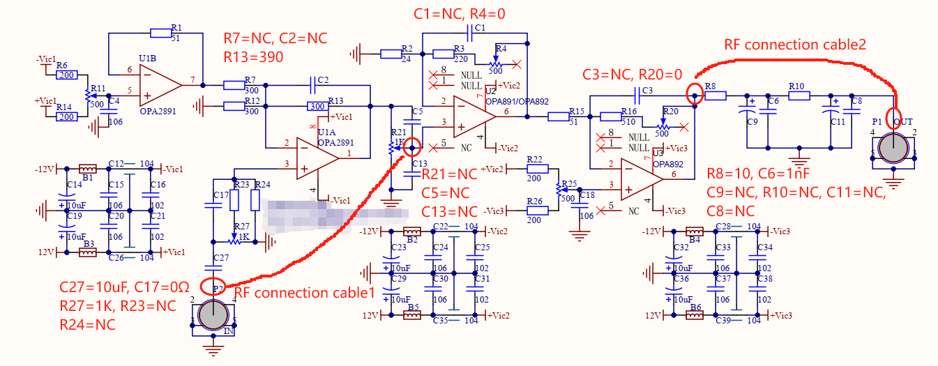
电路原理图如下所示:
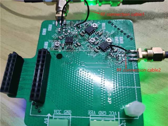
PCB实物图如下所示:
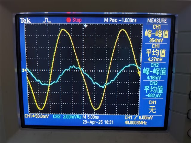
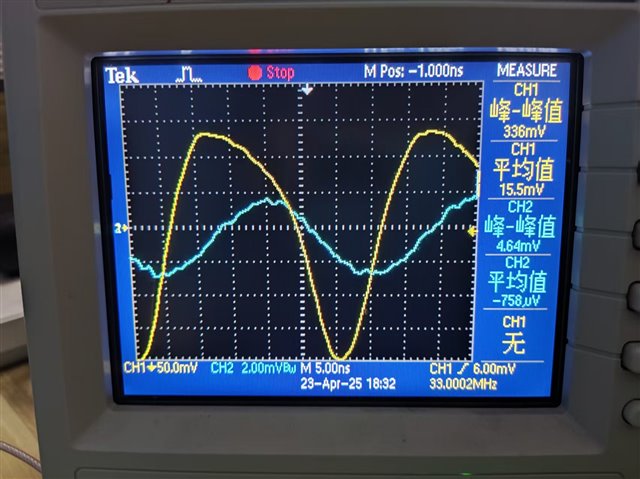
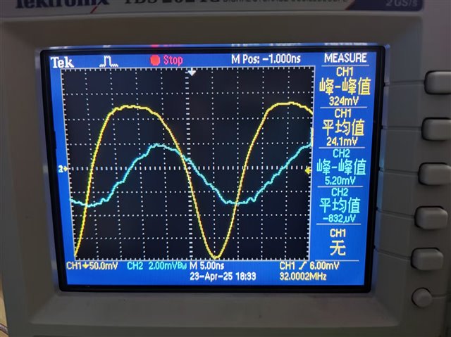
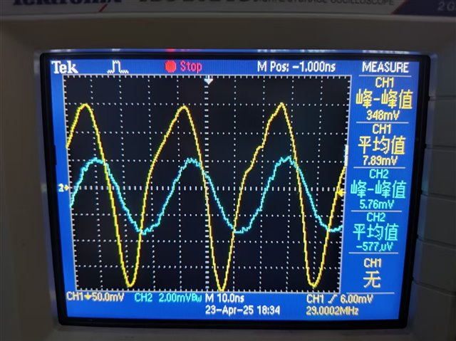
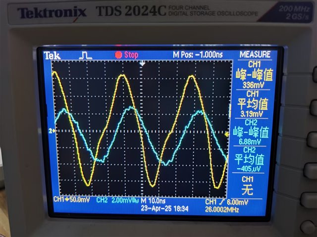
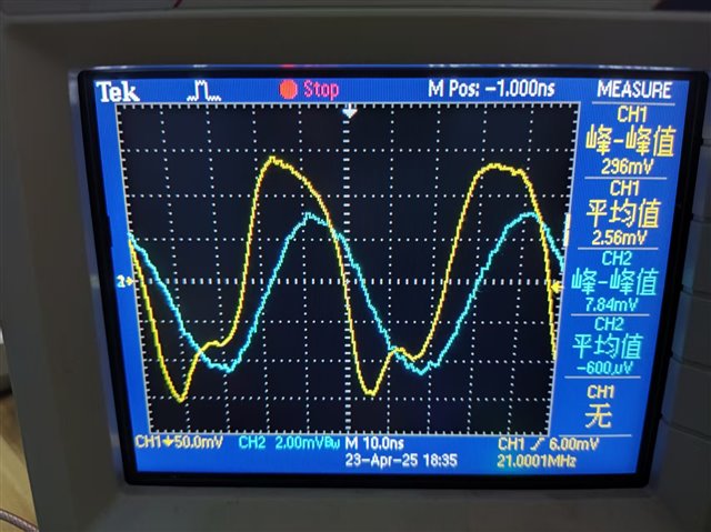
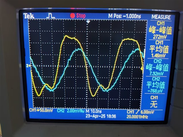
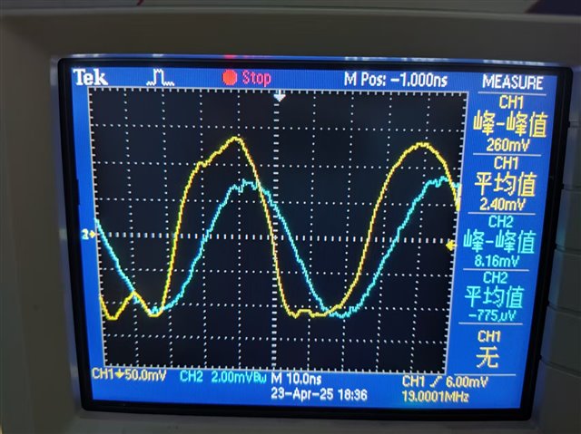
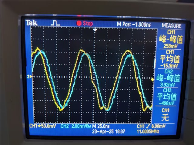
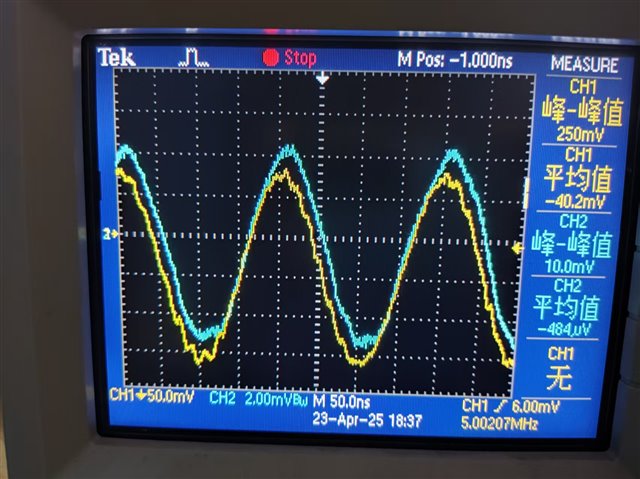
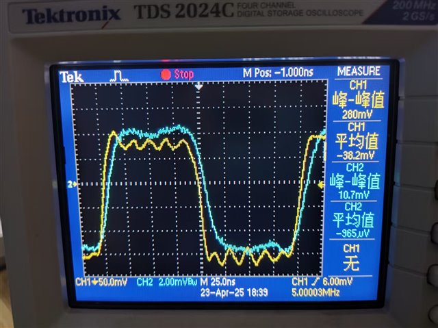
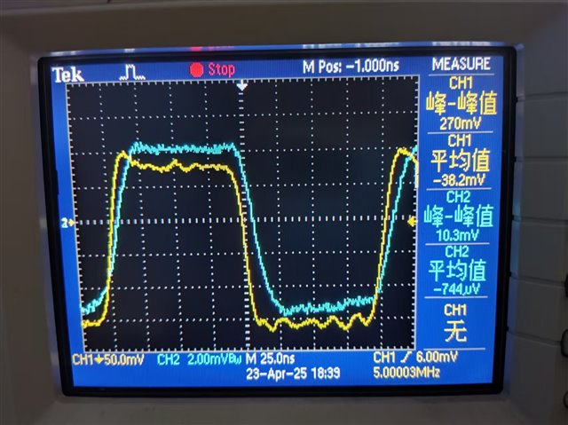
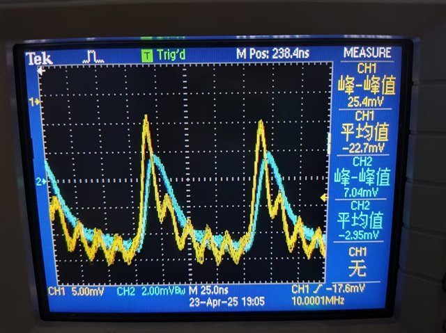
两根射频连接跳线是为了只测试板子上由两个 OPA892 构成的两级放大。不同频率的输入信号(蓝色)和放大后的输出信号(黄色_“打开反相”)如下所示:
感谢您对TI产品的关注!关于你的咨询,我们正在确认你的问题,稍后回复您。
由于您已经在英文论坛发帖,我们将在英文论坛回答这个问题。