This thread has been locked.

If you have a related question, please click the "Ask a related question" button in the top right corner. The newly created question will be automatically linked to this question.

寻求TLV320DAC3203支持-microphone DATA无输出CLK高点评

Other Parts Discussed in Thread: TLV320DAC3203, TLV320DAC3203EVM-K

TI 你好,

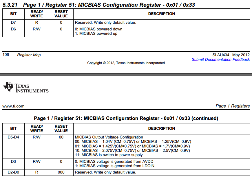
我们正在自己的板子上用TLV320DAC3203,碰到的问题是mic没有输入。MIC我们用的是admp421b,给它提供电源的MICBIAS 1.8v avdd,通过配置DAC寄存器0x33可改变电压。

有几个疑问,请一定帮忙。可否发邮件给我留一个电话?

1. MICBIAS可否通过LDOIN来得到,尝试配置过,但无法得到,即使在你们的demo板上。tlv320dac3203evm-K

2. MICBIAS如果通过avdd来得到,那么DAC3203的AVDD一定要外接1.8v吗?

3.如果AVDD外接1.8v, MICBIAS能正确提供电压,MIC的CLK和DATA该如何产生,需要DAC如何配置呢?当前是按照user guide里的配置如下:

#----------- Initialize to page 0
w 30 00 00
#----------- Initialize the device through software reset
w 30 01 01
#----------- Set PLL_CLKIN as MCLK and CODEC_CLKIN as PLL_CLK,
w 30 04 03
#----------- Power up pll, set pll divider P=1 and pll divider R=1,
w 30 05 91
#----------- Set pll divider J=8
w 30 06 08
#----------- Set pll divider D=0000
w 30 07 00
w 30 08 00
#----------- Power up and set NADC divider = 2,
w 30 12 82
#----------- Power up and set MDAC divider = 16
w 30 13 90
#----------- Set AOSR = 64
w 30 14 40
#----------- Select page 1
w 30 00 01
#----------- Disable internal crude AVdd in presence of external AVdd supply
#----------- or before powering up internal AVdd LDO
w 30 01 08
#----------- Enable master analog power control
w 30 02 00
#----------- Set the REF charging time to 40ms
w 30 7b 01
#----------- Select page 0
w 30 00 00
#----------- Select PRB_R2
w 30 3d 02
#----------- Configure MISO as clock output for digital microphone
w 30 37 0e
#----------- Power up left ADC and right ADC. Enable digital microphone mode for left ADC
#----------- and right ADC. Treat data on SCLK as digital microphone data
w 30 51 dc
#----------- Unmute left ADC and right ADC
w 30 52 0

  • 自己补充一下,I2S的几个主要CLK信号都有了,MCLK, BCLK, WCLK等。

    但Audio Line in始终没有。软件配置似乎没什么问题,请帮忙看下。谢谢

  • 1. MICBIAS可否通过LDOIN来得到,尝试配置过,但无法得到,即使在你们的demo板上。tlv320dac3203evm-K

    可以,设置下表中的对应位:

    设置D3为1,D6为1。

    2. MICBIAS如果通过avdd来得到,那么DAC3203的AVDD一定要外接1.8v吗?

    是的。

    3.如果AVDD外接1.8v, MICBIAS能正确提供电压,MIC的CLK和DATA该如何产生,需要DAC如何配置呢?

    MIC的Clk是由DAC3203给出的,Data是由MIC送给DAC3203的。

    下面是一个示例配置,请参考:

    ###############################################
    # Digital Microphone Script Loopback
    # ---------------------------------------------
    # Digital microphone data (DOUT) is sent to
    # the DAC's DIN pin internally. DOUT data
    # is also sent to the USB controller.
    ###############################################

    ###############################################
    # Software Reset
    ###############################################
    #
    # Select Page 0
    w 30 00 00
    #
    # Initialize the device through software reset
    w 30 01 01
    #
    ###############################################

    ###############################################
    # Clock and Interface Settings
    # ---------------------------------------------
    # The codec receives: MCLK = 11.2896 MHz,
    # WCLK = 44.1 kHz
    ###############################################
    #
    # Select Page 0
    w 30 00 00
    #
    # PLL_clkin = MCLK, codec_clkin = PLL_CLK,
    # PLL on, P=1, R=1, J=8, D=0000
    w 30 04 03 91 08 00 00
    #
    # NDAC = 2, MDAC = 8, dividers powered on
    w 30 0b 82 88
    #
    # DOSR = 128
    w 30 0D 00 80
    #
    # NADC = 2, MADC = 16, dividers powered on
    w 30 12 82 90
    #
    # AOSR = 64
    w 30 14 40
    #
    # Digital Loopback
    # Routes DOUT to DIN internally, DOUT pin
    # is still output, DIN pin is ignored
    w 30 1D 10
    #
    ###############################################

    ###############################################
    # Configure Power Supplies
    ###############################################
    #
    # Select Page 1
    w 30 00 01
    #
    # Disable weak AVDD in presence of external
    # AVDD supply
    w 30 01 08
    #
    # Enable Master Analog Power Control
    w 30 02 00
    #
    # Set the input power-up time to 3.1ms (for ADC)
    w 30 47 32
    #
    # Set the REF charging time to 40ms
    w 30 7b 01
    #
    ###############################################

    ###############################################
    # Configure Processing Blocks
    ###############################################
    #
    # Select Page 0
    w 30 00 00
    #
    # PRB_P2 and PRB_R2 selected
    w 30 3C 02 02
    #
    ################################################
    # High-pass first order Butterworth2 filter,
    # fc = 80 Hz
    ###############################################
    #
    # Write to Buffer A:
    #
    # BIQUAD A, Left Channel (Page 8, Register 36, C7-C11)
    w 30 00 08
    w 30 24 7E F8 EB 00 81 07 15 00 7E F8 EB 00 7E F7 DD 00 82 0C 0C 00
    #
    # BIQUAD A, Right Channel (Page 9, Register 44, C39-C43)
    w 30 00 09
    w 30 2c 7E F8 EB 00 81 07 15 00 7E F8 EB 00 7E F7 DD 00 82 0C 0C 00
    #
    # Write to Buffer B:
    #
    # BIQUAD A, Left Channel (Page 26, Register 36, C7-C11)
    w 30 00 1A
    w 30 24 7E F8 EB 00 81 07 15 00 7E F8 EB 00 7E F7 DD 00 82 0C 0C 00
    #
    # BIQUAD A, Right Channel (Page 27, Register 44, C39-C43)
    w 30 00 1B
    w 30 2c 7E F8 EB 00 81 07 15 00 7E F8 EB 00 7E F7 DD 00 82 0C 0C 00
    #
    ###############################################


    ###############################################
    # Configure ADC Channel
    ###############################################
    #
    # Select Page 0
    w 30 00 00
    #
    # Configure MISO as clock output for DIGMIC
    w 30 37 0E
    #
    # LADC and RADC enabled for DIGMIC
    # Route SCLK as DIGMIC_DATA
    # Power up LADC/RADC
    w 30 51 DC
    #
    # Unmute LADC/RADC
    w 30 52 00
    #
    ###############################################

    ###############################################
    # Configure DAC Channel
    ###############################################
    #
    # Select Page 1
    w 30 00 01
    #
    # De-pop: 5 time constants, 6k resistance
    w 30 14 25
    #
    # Route LDAC/RDAC to HPL/HPR
    w 30 0c 08 08
    #
    # Select Page 0
    w 30 00 00
    #
    # DAC => 0dB
    w 30 41 00 00
    #
    # Power up LDAC/RDAC
    w 30 3f d6
    #
    # Select Page 1
    w 30 00 01
    #
    # Unmute HPL/HPR driver, 0dB Gain
    w 30 10 00 00
    #
    # Power up HPL/HPR
    w 30 09 30
    #
    # Select Page 0
    w 30 00 00
    #
    # Unmute LDAC/RDAC
    w 30 40 00
    #
    ###############################################

  • 你好,请问你有这个的参考驱动吗?