This thread has been locked.
If you have a related question, please click the "Ask a related question" button in the top right corner. The newly created question will be automatically linked to this question.
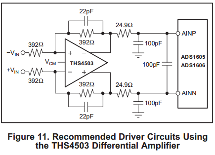
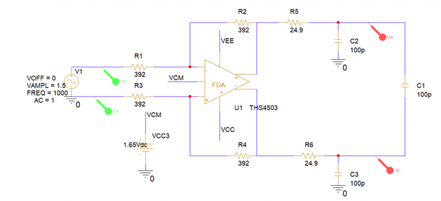
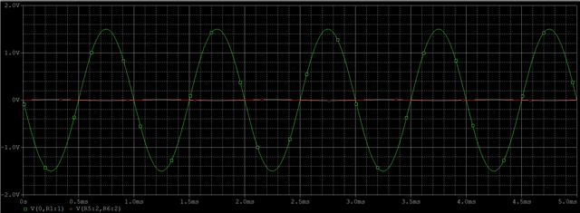
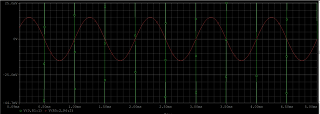
输入信号Vin幅值±3V,希望借由Figure10所示电路实现单端转差分,但实现Vin/2和-Vin/2(两路信号需要完全同步)有困难且需要尽量少的噪声,所以采用Figure10所示电路,并在Pspice中搭建了示例电路,但不知道用法何处不对,其输出结果被衰减至±15mV左右。
您好,
仿真时供电电压是多少?请注意 THS4503的供电范围以及输入输出范围。
供电电压为±5V,输入±1.5V,希望输出差模1.5V、共模1.65V的信号,以上仿真条件均满足技术手册参数(±5V供电范围下的输入共模范围为±4V,输出电压摆幅±8V)
已解决,仿真初始条件不可跳过。
很高兴您的问题得到解决,感谢您的反馈