If you have a related question, please click the "Ask a related question" button in the top right corner. The newly created question will be automatically linked to this question.
The Full-Scale Input voltage is a function of the Programmable Gain Amplifier (PGA gain setting) and the voltage Reference used for conversion. In general, the user will select the PGA Gain so the differential input signal does not exceed the Full-Scale Input voltage. The differential input voltage is the difference of the positive and negative input voltage:
VINdifferential = AINP – AINN equation(1)
The full-scale input voltage is defined by the equation:
Full-scale input voltage = +/-VREF/PGAGAIN equation(2)
2) Common-Mode Input Voltage Range
The ADS1146/7/8 and ADS1246/7/8 common-mode input voltage range is a function of the AVDD and AVSS supplies, the PGA gain setting and the differential voltage applied to the inputs. The common-mode voltage range must be met in order to provide the internal PGA with the necessary headroom to remain in its linear range of operation. The common-mode voltage is the average voltage of the positive and negative inputs:
VCM = (AINP+AINN)/2 equation(3)
The input common-mode voltage range is delimited by the following equation:
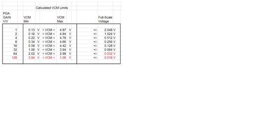
- Example 1. A typical application is to measure an ungrounded thermocouple using a uni-polar supply configuration with AVSS =0V and AVDD=+5V. The thermocouple common-mode voltage could be set using the internal bias generator function (VBIAS). The internal bias generator provides a voltage VBIAS in the middle of the supplies (AVDD+AVSS)/2. This voltage may be applied to one of the inputs connected to the ungrounded thermocouple. When the VBIAS function is used, the common-mode voltage is set at an optimal point, providing more headroom for larger differential signals and for the use of larger PGA gain settings. The bias voltage generation function (VBIAS) is described on the ADS1246/7/8 datasheet on page 29 and on the ADS1146/7/8 datasheet on page 20. For example, if the maximum expected differential voltage from a K-type thermocouple is ~60mV; the allowed Common-Mode Voltage range limits Vs. PGA Gain can be calculated using equation (4). In addition, the full-scale voltage can be calculated using equation (2):
Conditions :
AVDD = 5V, AVSS = 0V, VREF = 2.048V;
AINP=2.560 V
AINN= (AVDD-AVSS)/2 = 2.5V (connected to VBIAS)
VINdifferential = AINP –AINN = +0.060V
VCM = (AINP+AINN)/2 = 2.530
Looking at the table above, the user may not use the PGA Gain of 64 or 128; since the 60mV differential signal exceeds the full-scale differential voltage. In addition, in this case, the user runs out of headroom on the common mode voltage range when the PGA gain is set to GAIN=128.
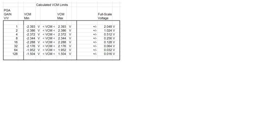
- Example 2. In some applications, the user may need to make a measurement that is single-ended or referred to GND. Since the internal PGA of the device requires a minimum common-mode voltage above the AVSS supply, the user is required to set up the device using bi-polar supplies, +AVDD and –AVSS. A common application is to measure a grounded thermocouple. In this case, the device may be set up with AVDD=2.5V and AVSS=-2.5V. If we assume, for this example, that the maximum expected differential voltage for a type B thermocouple is ~14mV; the allowed Common-Mode Voltage range limits Vs. PGA Gain can be calculated using equation (4). In addition, the full-scale voltage can be calculated using equation (2):
Conditions :
AVDD = +2.5V, AVSS = -2.5V, VREF = 2.048V
AINP = +14 mV
AINN = GND (Thermocouple is grounded)
VINdifferential = AINP –AINN = +0.014V
VCM = (AINP+AINN)/2 = +0.007V
In this example, since the maximum expected differential signal is 14mV; the user may use Gain=128 without exceeding the +/-16mV full-scale voltage. In addition, in this example, the common-mode voltage of 7mV is inside the allowed common-mode range for all PGA Gain cases.