

Other Parts Discussed in Thread: ADC108S022
是用的是SPI接口的ADC芯片,时序如下
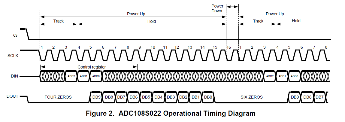
DOUT :The output samples are clocked out of this pin on the falling edges of the SCLK pin
DIN THE ADC108S022's Control Register is loaded through this pin on rising edges of the SCLK pin
是不是说,DIN是在SCLK上升沿向ADC写参数,而DOUT在SCLK的下降沿从ADC中读取转换后的数据??
