

我有一个在三个不同的电路板上运行的超低功耗应用、2个使用 TM4C123GH6PGEI 144引脚、最新的使用 TM4C123GH6PMIR 64引脚。 I2C0位于同一引脚多路复用引脚上。
该应用需要外部低功耗存储器来存储易失性状态变量和"采样 num"等内容。 片上 EEPROM 不是一个选项、因为我们的部署持续一年以上、远远超过了额定的50万写入周期。 我已经尝试过 HIB 模块 RAM、但是、我们希望存储的内容要多于 HIB RAM 可以容纳的内容、因此我们使用了 FRAM。
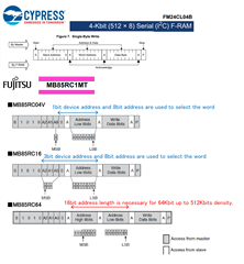
前两个电路板使用 Cypress FRAM FM24CL04B、后者具有单字节寄存器地址、最新电路板使用更大的 Fujitsu MB85RC1MTPNF FRAM、因为我们计划缓存样本数据、然后 以突发块的方式写入外部 NAND 闪存或 microSD。
用于较小4KB FRAM 的 I2C 驱动程序工作正常。 我的问题是如何为更大的128KB Fujitsu FRAM 写入两个字节的地址。 该图显示了 i2c 字节序列。
我的 Cypress 的 i2c 驱动程序对 rom_i2cmasterdataaput 进行了一次调用... 我要做的是如下所示:
//将要写入的地址放在数据寄存器中。
#if Fujitsu_BIGFRAM = 1.
ROM_I2CMasterDataPut (I2C0_BASE、(uint8_t)(ucStart_addr/256));
#endif
ROM_I2CMasterDataPut (I2C0_BASE、(uint8_t) ucStart_addr);
这是不正确的(因为它不起作用)、但我看不到16位(2字节) API。 请提供有关如何执行两个字节地址的建议。 我在 e2e 论坛上看到过其他帖子、但没有答案。
谢谢
void fram_test(void)
{
    int indx;

    uprintf("\r\n1st block of 128, write 127 to 0\r\n");
    for(indx=0; indx<128; indx++)               // 0->127
        framBuf[indx] = 127-indx;
    i2c0_write(I2C_FRAM_ADDR, framBuf, 128, 0x00);
    for(indx=0; indx<128; indx++)
    {
        uprintf("%02x ", framBuf[indx]);
        if(indx%16 == 0x0f)
            uprintf("\r\n");
    }

    uprintf("\r\n2nd block of 128, write 0 to 127\r\n");
    for(indx=0; indx<128; indx++)
        framBuf[indx] = indx;
    i2c0_write(I2C_FRAM_ADDR, framBuf, 128, 128);
    for(indx=0; indx<128; indx++)
    {
        uprintf("%02x ", framBuf[indx]);
        if(indx%16 == 0x0f)
            uprintf("\r\n");
    }

    wait_consoleTx();

    uprintf("\r\n3rd block of 128, write 255 to 128\r\n");
    for(indx=0; indx<128; indx++)
        framBuf[indx] = 255-indx;
    i2c0_write(I2C_FRAM_ADDR, framBuf, 128, 256);
    for(indx=0; indx<128; indx++)
    {
        uprintf("%02x ", framBuf[indx]);
        if(indx%16 == 0x0f)
            uprintf("\r\n");
    }

    uprintf("\r\n4th block of 128, write 128 to 255\r\n");
    for(indx=0; indx<128; indx++)
        framBuf[indx] = 128+indx;
    i2c0_write(I2C_FRAM_ADDR, framBuf, 128, 384);
    for(indx=0; indx<128; indx++)
    {
        uprintf("%02x ", framBuf[indx]);
        if(indx%16 == 0x0f)
            uprintf("\r\n");
    }

    wait_consoleTx();

    for(indx=0; indx<128; indx++)
        framBuf[indx] = 0x55;


    uprintf("\r\n1st block of 128, read:\r\n");
    i2c0_read(I2C_FRAM_ADDR, framBuf, 128, 0, FALSE);
    for(indx=0; indx<128; indx++)
    {
        uprintf("%02x ", framBuf[indx]);
        if(indx%16 == 0x0f)
            uprintf("\r\n");
    }

    uprintf("\r\n2nd block of 128, read:\r\n");
    i2c0_read(I2C_FRAM_ADDR, framBuf, 128, 128, FALSE);
    for(indx=0; indx<128; indx++)
    {
        uprintf("%02x ", framBuf[indx]);
        if(indx%16 == 0x0f)
            uprintf("\r\n");
    }

    wait_consoleTx();

    uprintf("\r\n3rd block of 128, read:\r\n");
    //i2c0_read(I2C_FRAM_ADDR|0x01, framBuf, 128, 256, FALSE);
    i2c0_read(I2C_FRAM_ADDR, framBuf, 128, 256, FALSE);
    for(indx=0; indx<128; indx++)
    {
        uprintf("%02x ", framBuf[indx]);
        if(indx%16 == 0x0f)
            uprintf("\r\n");
    }

    uprintf("\r\n4th block of 128, read:\r\n");
    i2c0_read(I2C_FRAM_ADDR, framBuf, 128, 384, FALSE);
    for(indx=0; indx<128; indx++)
    {
        uprintf("%02x ", framBuf[indx]);
        if(indx%16 == 0x0f)
            uprintf("\r\n");
    }

    wait_consoleTx();

}

/******************************************************************************
 * Initialize and configure I2C module in TIVA tm4c123gh6pge
 *            MFET uses I2C0_BASE on PB2/PB3, the other i2c periph base addr are not used
 *
 * Parameters:
 *          ui32Base: I2Cx base address. The address is one of the following values:
 *              I2C0_BASE, I2C1_BASE, I2C2_BASE, I2C3_BASE.
 *
 *      bFast:
 *              true : I2C will run in fast mode (400kbps)
 *              false: I2C will run in standard mode (100kbps)
 *
 * Return: none
 *****************************************************************************/
void i2c0_init(bool bFast)
{

    //ROM_SysCtlPeripheralEnable(SYSCTL_PERIPH_GPIOB);      // this is done prior in init.c

    //enable onchip I2C peripheral
    ROM_SysCtlPeripheralEnable(SYSCTL_PERIPH_I2C0);

    //reset I2C module
    ROM_SysCtlPeripheralReset(SYSCTL_PERIPH_I2C0);

    // Configure the pin muxing for I2C0 functions on port PB2(SCL) and PB3(SDA).
    ROM_GPIOPinConfigure(GPIO_PB2_I2C0SCL);     // This is the same on 144 pin part and 64pin part
    ROM_GPIOPinConfigure(GPIO_PB3_I2C0SDA);

    // Configure the appropriate pins to be I2C instead of GPIO.
    ROM_GPIOPinTypeI2C(GPIO_PORTB_BASE, GPIO_PIN_2 | GPIO_PIN_3);
    //GPIOPinTypeI2CSCL(GPIO_PORTB_BASE, GPIO_PIN_2);
    //GPIOPinTypeI2C(GPIO_PORTB_BASE, GPIO_PIN_3);


    ROM_GPIOPadConfigSet(GPIO_PORTB_BASE, GPIO_PIN_2, GPIO_STRENGTH_2MA, GPIO_PIN_TYPE_STD);
    ROM_GPIOPadConfigSet(GPIO_PORTB_BASE, GPIO_PIN_3, GPIO_STRENGTH_2MA, GPIO_PIN_TYPE_OD);

    // Initialize the I2C master - Transfer speed is defined depend on variable bFast
    ROM_I2CMasterInitExpClk(I2C0_BASE, SysCtlClockGet(), bFast);

    //clear I2C FIFOs
    HWREG(I2C0_BASE + I2C_O_FIFOCTL) = 80008000;

    ROM_I2CMasterEnable(I2C0_BASE);      //I2C is ready to use

}

/******************************************************************************
 * Write multiple bytes to a slave device
 *
 * Parameters:
 *  uiSlave_addr : the slave address
 *  *ucData    : the data that are going to be sent
 *  uiCount    : number of byte will be sent
 *  ucStart_addr : register address you want to write or a control byte
 *
 * Return: none
 * Useful info:  github.com/.../FRAM_MB85RC_I2C
 *****************************************************************************/
void i2c0_write(unsigned char uiSlave_addr, unsigned char *ucData, uint16_t uiCount, uint16_t ucStart_addr)  //void i2c0_write(unsigned char uiSlave_add, unsigned char *ucData, uint16_t uiCount, unsigned char ucStart_add)
{
    unsigned int temp = 1;
    IntMasterDisable();

    // Set the slave address and setup for a transmit operation.
    ROM_I2CMasterSlaveAddrSet(I2C0_BASE, uiSlave_addr, false);

    // Place the address to be written in the data register.
#if FUJITSU_BIGFRAM == 1      // This does not work, need to find a two byte API
    ROM_I2CMasterDataPut(I2C0_BASE, (uint8_t)(ucStart_addr/256));
#endif
    ROM_I2CMasterDataPut(I2C0_BASE, (uint8_t)ucStart_addr);

    while (ROM_I2CMasterBusy(I2C0_BASE));
    if (uiCount == 0)
        // Initiate send of character from Master to Slave
        ROM_I2CMasterControl(I2C0_BASE, I2C_MASTER_CMD_SINGLE_SEND);
    else
    {
        // Start the burst cycle, writing the address as the first byte.
        ROM_I2CMasterControl(I2C0_BASE, I2C_MASTER_CMD_BURST_SEND_START);
        // Write the next byte to the data register.
        while (ROM_I2CMasterBusy(I2C0_BASE));
        ROM_I2CMasterDataPut(I2C0_BASE, ucData[0]);
        for( ; temp < uiCount; temp++)        //Loop to send data if not the last byte
        {
            // Continue the burst write.
            ROM_I2CMasterControl(I2C0_BASE, I2C_MASTER_CMD_BURST_SEND_CONT);
            // Write the next byte to the data register.
            while (ROM_I2CMasterBusy(I2C0_BASE));
            ROM_I2CMasterDataPut(I2C0_BASE, ucData[temp]);
        }
        // Finish the burst write.
        ROM_I2CMasterControl(I2C0_BASE, I2C_MASTER_CMD_BURST_SEND_FINISH);
    }
    while (ROM_I2CMasterBusy(I2C0_BASE));
    IntMasterEnable();
}

/******************************************************************************
 * Read multiple bytes from slave device
 *
 * Parameters:
 *  uiSlave_addr: the slave address
 *  *ucRec_Data: a variable to save the data received
 *  uiCount    : number of byte will be received
 *  ucStart_addr: register address you want to read or a control byte (Bug fix 9/9/2022:  NanoFET has large 128KB FRAM, according to Fujitsu datasheet, large FRAM requires 2 bytes of address)
 *
 * Return: none
 *****************************************************************************/
void i2c0_read(unsigned char uiSlave_addr, unsigned char *ucRec_Data, uint16_t uiCount, uint16_t ucStart_addr, bool bDummyRead)   //void I2C_Read(uint32_t ui32Base, unsigned char uiSlave_add, unsigned char *ucRec_Data, uint16_t uiCount, unsigned char ucStart_add, bool bDummyRead)
{
    unsigned int uitemp = 0;
        // Set the slave address and setup for a transmit operation.

    IntMasterDisable();
    ROM_I2CMasterSlaveAddrSet(I2C0_BASE, uiSlave_addr, false);

    // Place the address to be written in the data register.
#if FUJITSU_BIGFRAM == 1      // This does not work, need to find a two byte API
    ROM_I2CMasterDataPut(I2C0_BASE, (uint8_t)(ucStart_addr/256));
#endif
    ROM_I2CMasterDataPut(I2C0_BASE, (uint8_t)ucStart_addr);

    // Start the burst cycle, writing the address as the first byte.
    ROM_I2CMasterControl(I2C0_BASE, I2C_MASTER_CMD_BURST_SEND_START);

    while (ROM_I2CMasterBusy(I2C0_BASE))
        ;
        //while (!(ROM_I2CMasterErr(ui32Base) == I2C_MASTER_ERR_NONE));

    ROM_I2CMasterSlaveAddrSet(I2C0_BASE, uiSlave_addr, true);
    if (uiCount == 1)
    {
        ROM_I2CMasterControl(I2C0_BASE, I2C_MASTER_CMD_SINGLE_RECEIVE);
        while (ROM_I2CMasterBusy(I2C0_BASE));
        ucRec_Data[0]  = ROM_I2CMasterDataGet(I2C0_BASE);
        if (bDummyRead)
        {
            while (ROM_I2CMasterBusy(I2C0_BASE));
            ucRec_Data[0]  = ROM_I2CMasterDataGet(I2C0_BASE);
        }
    }
    else
    {
        ROM_I2CMasterControl(I2C0_BASE, I2C_MASTER_CMD_BURST_RECEIVE_START);
        if (bDummyRead)
        {
            while (ROM_I2CMasterBusy(I2C0_BASE))
                ;
            ucRec_Data[0]  = ROM_I2CMasterDataGet(I2C0_BASE);
        }
        while (ROM_I2CMasterBusy(I2C0_BASE))
            ;
        ucRec_Data[uitemp++]  = ROM_I2CMasterDataGet(I2C0_BASE);
        for ( ; uitemp < (uiCount - 1); uitemp++)
        {
            ROM_I2CMasterControl(I2C0_BASE, I2C_MASTER_CMD_BURST_RECEIVE_CONT);
            while (ROM_I2CMasterBusy(I2C0_BASE))
                ;
            ucRec_Data[uitemp]  = ROM_I2CMasterDataGet(I2C0_BASE);
        }
        ROM_I2CMasterControl(I2C0_BASE, I2C_MASTER_CMD_BURST_RECEIVE_FINISH);
        while (ROM_I2CMasterBusy(I2C0_BASE))
            ;
        ucRec_Data[uitemp]  = ROM_I2CMasterDataGet(I2C0_BASE);
    }

    while (ROM_I2CMasterBusy(I2C0_BASE))
        ;
    IntMasterEnable();
}
