This thread has been locked.

If you have a related question, please click the "Ask a related question" button in the top right corner. The newly created question will be automatically linked to this question.

[参考译文] TM4C1290NCZAD:用于 xtal 和相关 GNDING 的 BGA 封装 PCB 布局。

Guru**** 2502205 points
Other Parts Discussed in Thread: TM4C1290NCZAD

请注意,本文内容源自机器翻译,可能存在语法或其它翻译错误,仅供参考。如需获取准确内容,请参阅链接中的英语原文或自行翻译。

https://e2e.ti.com/support/microcontrollers/arm-based-microcontrollers-group/arm-based-microcontrollers/f/arm-based-microcontrollers-forum/1163194/tm4c1290nczad-bga-package-pcb-layout-for-xtal-and-associated-gnding

器件型号:TM4C1290NCZAD

大家好、TM4C 团队、

我的客户有以下问题...  

使用 TI TM4C1290NCZAD 微控制器..

系统设计指南要求使用 GNDX 引脚将晶体电路接地、但我们使用的是 BGA 封装、该封装将这些 GNDX 焊球放置在非常特殊的位置、以便能够在信号线路之间提供 GND。 设计指南表明这是可能的。

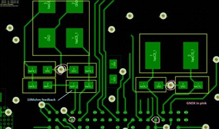
我现在附上了 PCB 的屏幕截图(请参阅下面的 SNIP)。 粉色圆圈是 GNDX 位置。

我们在高频晶体上添加了一个10M Ω 反馈电阻器、以防万一。 即使没有它、路由也会被阻止。

我 见过这个参考布局。   [ http://www.ti.com/lit/zip/tidc246 ]并浏览了“TM4C129x 系列 Tiva C 系列微控制器的系统设计指南”。  http://www.ti.com/lit/an/spma056/spma056.pdf。 

对此有一些建议吗?  谢谢!

谢谢、Merril

  • 请注意,本文内容源自机器翻译,可能存在语法或其它翻译错误,仅供参考。如需获取准确内容,请参阅链接中的英语原文或自行翻译。

    您好!

     我不是 PCB 布局专家。 我看到 GNDX2 (焊球 D18)被带到一个连接到数字接地的过孔、而两个电容器被连接到另一个连接到接地的过孔。 对我来说没关系。