This thread has been locked.

If you have a related question, please click the "Ask a related question" button in the top right corner. The newly created question will be automatically linked to this question.

[参考译文] TM4C1233E6PM:ADC 读数错误

Guru**** 2379300 points
请注意,本文内容源自机器翻译,可能存在语法或其它翻译错误,仅供参考。如需获取准确内容,请参阅链接中的英语原文或自行翻译。

https://e2e.ti.com/support/microcontrollers/arm-based-microcontrollers-group/arm-based-microcontrollers/f/arm-based-microcontrollers-forum/1367984/tm4c1233e6pm-incorrect-reading-on-adc

器件型号:TM4C1233E6PM
主题中讨论的其他器件:SEGGER

工具与软件:

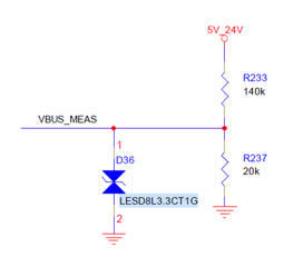
我在 tm4c12433 MCU 上的 ADC 通道11一直存在问题。 即使未施加电压、我始终读出890的原始值(阶跃计数)。 理想情况下、它应将零读取为原始值。

以下是详细信息:
-** mc:** tm4c12433
-**晶体振荡器(Xtal):** 6 MHz

我已经确保将这些引脚作为 ADC 正确启用。 以下是我用于从 ADC 通道11读取的配置:

#define VBUS_MEAS_ADC_BASE GPIO_PORTB_BASE
#define VBUS_MEAS_ADC_PIN GPIO_PIN_5

GPIOPinTypeADC (VBUS_MEAS_ADC_BASE、VBUS_MEAS_ADC_PIN);
GPIOPinTypeGPIOInput (VBUS_MEAS_ADC_BASE、VBUS_MEAS_ADC_PIN);

uint32_t uiReadVbusVoltage (void)
{
uint32_t ADCValues[1];

ADCSequenceConfigure (ADC0_BASE、3、ADC_TRIGGER_processor、0);
ADCSequenceStepConfigure (ADC0_BASE、3、0、ADC_CTL_CH11 | ADC_CTL_IE | ADC_CTL_END);
ADCSequenceEnable (ADC0_BASE、3);
ADCIntClear (ADC0_BASE、3);


while (1)
{
//
///触发 ADC 转换
//
ADCProcessorTrigger (ADC0_BASE、3);

//
//等待转换完成。
//
while (! ADCIntStatus (ADC0_BASE、3、false)
{

//
//清除 ADC 中断标志。
//
ADCIntClear (ADC0_BASE、3);

//
//读取 ADC 值。
//
ADCSequenceDataGet (ADC0_BASE、3、ADCValues);


SEGGR_RTT_printf (0、"原始样本(ADCValues[0]):%04d\r"、ADCValues[0]);


//
//该函数提供了一种生成恒定长度的方法
//延迟。 函数延迟(以周期为单位)= 3 *参数。 延迟
//任意250ms。
//
SysCtlDelay (80000000 / 12);


输出打印如下:
原始样本(ADCValues[0]):0891

您能否帮助我确定可能导致此问题的原因?

  • 请注意,本文内容源自机器翻译,可能存在语法或其它翻译错误,仅供参考。如需获取准确内容,请参阅链接中的英语原文或自行翻译。

    您好!

     我在 LaunchPad 上尝试了 AIN11、但我无法重现您的结果。 为什么不先在 LaunchPad 上尝试我的代码、然后在您的定制板上尝试。 我将 PB5 (AIN11)连接到 GND 或3.3V、并且我可以看到 ADC 值等于0或4095。  

    #include <stdbool.h>
    #include <stdint.h>
    #include "inc/hw_memmap.h"
    #include "driverlib/adc.h"
    #include "driverlib/gpio.h"
    #include "driverlib/pin_map.h"
    #include "driverlib/sysctl.h"
    #include "driverlib/uart.h"
    #include "utils/uartstdio.h"
    
    //*****************************************************************************
    //
    //! \addtogroup adc_examples_list
    //! <h1>Single Ended ADC (single_ended)</h1>
    //!
    //! This example shows how to setup ADC0 as a single ended input and take a
    //! single sample on AIN11/PE3.
    //!
    //! This example uses the following peripherals and I/O signals.  You must
    //! review these and change as needed for your own board:
    //! - ADC0 peripheral
    //! - GPIO Port E peripheral (for AIN11 pin)
    //! - AIN11 - PE3
    //!
    //! The following UART signals are configured only for displaying console
    //! messages for this example.  These are not required for operation of the
    //! ADC.
    //! - UART0 peripheral
    //! - GPIO Port A peripheral (for UART0 pins)
    //! - UART0RX - PA0
    //! - UART0TX - PA1
    //!
    //! This example uses the following interrupt handlers.  To use this example
    //! in your own application you must add these interrupt handlers to your
    //! vector table.
    //! - None.
    //
    //*****************************************************************************
    
    //*****************************************************************************
    //
    // This function sets up UART0 to be used for a console to display information
    // as the example is running.
    //
    //*****************************************************************************
    void
    InitConsole(void)
    {
        //
        // Enable GPIO port A which is used for UART0 pins.
        // TODO: change this to whichever GPIO port you are using.
        //
        SysCtlPeripheralEnable(SYSCTL_PERIPH_GPIOA);
    
        //
        // Configure the pin muxing for UART0 functions on port A0 and A1.
        // This step is not necessary if your part does not support pin muxing.
        // TODO: change this to select the port/pin you are using.
        //
        GPIOPinConfigure(GPIO_PA0_U0RX);
        GPIOPinConfigure(GPIO_PA1_U0TX);
    
        //
        // Enable UART0 so that we can configure the clock.
        //
        SysCtlPeripheralEnable(SYSCTL_PERIPH_UART0);
    
        //
        // Use the internal 16MHz oscillator as the UART clock source.
        //
        UARTClockSourceSet(UART0_BASE, UART_CLOCK_PIOSC);
    
        //
        // Select the alternate (UART) function for these pins.
        // TODO: change this to select the port/pin you are using.
        //
        GPIOPinTypeUART(GPIO_PORTA_BASE, GPIO_PIN_0 | GPIO_PIN_1);
    
        //
        // Initialize the UART for console I/O.
        //
        UARTStdioConfig(0, 115200, 16000000);
    }
    
    //*****************************************************************************
    //
    // Configure ADC0 for a single-ended input and a single sample.  Once the
    // sample is ready, an interrupt flag will be set.  Using a polling method,
    // the data will be read then displayed on the console via UART0.
    //
    //*****************************************************************************
    int
    main(void)
    {
    #if defined(TARGET_IS_TM4C129_RA0) ||                                         \
        defined(TARGET_IS_TM4C129_RA1) ||                                         \
        defined(TARGET_IS_TM4C129_RA2)
        uint32_t ui32SysClock;
    #endif
    
        //
        // This array is used for storing the data read from the ADC FIFO. It
        // must be as large as the FIFO for the sequencer in use.  This example
        // uses sequence 3 which has a FIFO depth of 1.  If another sequence
        // was used with a deeper FIFO, then the array size must be changed.
        //
        uint32_t pui32ADC0Value[1];
    
        //
        // Set the clocking to run at 20 MHz (200 MHz / 10) using the PLL.  When
        // using the ADC, you must either use the PLL or supply a 16 MHz clock
        // source.
        // TODO: The SYSCTL_XTAL_ value must be changed to match the value of the
        // crystal on your board.
        //
    #if defined(TARGET_IS_TM4C129_RA0) ||                                         \
        defined(TARGET_IS_TM4C129_RA1) ||                                         \
        defined(TARGET_IS_TM4C129_RA2)
        //
        // Note: SYSCTL_CFG_VCO_240 is a new setting provided in TivaWare 2.2.x and
        // later to better reflect the actual VCO speed due to SYSCTL#22.
        //
        ui32SysClock = SysCtlClockFreqSet((SYSCTL_XTAL_25MHZ |
                                           SYSCTL_OSC_MAIN |
                                           SYSCTL_USE_PLL |
                                           SYSCTL_CFG_VCO_240), 20000000);
    #else
        SysCtlClockSet(SYSCTL_SYSDIV_10 | SYSCTL_USE_PLL | SYSCTL_OSC_MAIN |
                       SYSCTL_XTAL_16MHZ);
    #endif
    
        //
        // Set up the serial console to use for displaying messages.  This is
        // just for this example program and is not needed for ADC operation.
        //
        InitConsole();
    
        //
        // Display the setup on the console.
        //
        UARTprintf("ADC ->\n");
        UARTprintf("  Type: Single Ended\n");
        UARTprintf("  Samples: One\n");
        UARTprintf("  Update Rate: 250ms\n");
        UARTprintf("  Input Pin: AIN11/PE3\n\n");
    
        //
        // The ADC0 peripheral must be enabled for use.
        //
        SysCtlPeripheralEnable(SYSCTL_PERIPH_ADC0);
    
        //
        // For this example ADC0 is used with AIN11 on port B5.
        // The actual port and pins used may be different on your part, consult
        // the data sheet for more information.  GPIO port E needs to be enabled
        // so these pins can be used.
        // TODO: change this to whichever GPIO port you are using.
        //
        SysCtlPeripheralEnable(SYSCTL_PERIPH_GPIOB);
    
        //
        // Select the analog ADC function for these pins.
        // Consult the data sheet to see which functions are allocated per pin.
        // TODO: change this to select the port/pin you are using.
        //
        GPIOPinTypeADC(GPIO_PORTB_BASE, GPIO_PIN_5);
    
        //
        // Enable sample sequence 3 with a processor signal trigger.  Sequence 3
        // will do a single sample when the processor sends a signal to start the
        // conversion.  Each ADC module has 4 programmable sequences, sequence 0
        // to sequence 3.  This example is arbitrarily using sequence 3.
        //
        ADCSequenceConfigure(ADC0_BASE, 3, ADC_TRIGGER_PROCESSOR, 0);
    
        //
        // Configure step 0 on sequence 3.  Sample channel 0 (ADC_CTL_CH0) in
        // single-ended mode (default) and configure the interrupt flag
        // (ADC_CTL_IE) to be set when the sample is done.  Tell the ADC logic
        // that this is the last conversion on sequence 3 (ADC_CTL_END).  Sequence
        // 3 has only one programmable step.  Sequence 1 and 2 have 4 steps, and
        // sequence 0 has 8 programmable steps.  Since we are only doing a single
        // conversion using sequence 3 we will only configure step 0.  For more
        // information on the ADC sequences and steps, reference the datasheet.
        //
        ADCSequenceStepConfigure(ADC0_BASE, 3, 0, ADC_CTL_CH11 | ADC_CTL_IE |
                                 ADC_CTL_END);
    
        //
        // Since sample sequence 3 is now configured, it must be enabled.
        //
        ADCSequenceEnable(ADC0_BASE, 3);
    
        //
        // Clear the interrupt status flag.  This is done to make sure the
        // interrupt flag is cleared before we sample.
        //
        ADCIntClear(ADC0_BASE, 3);
    
        //
        // Sample AIN11 forever.  Display the value on the console.
        //
        while(1)
        {
            //
            // Trigger the ADC conversion.
            //
            ADCProcessorTrigger(ADC0_BASE, 3);
    
            //
            // Wait for conversion to be completed.
            //
            while(!ADCIntStatus(ADC0_BASE, 3, false))
            {
            }
    
            //
            // Clear the ADC interrupt flag.
            //
            ADCIntClear(ADC0_BASE, 3);
    
            //
            // Read ADC Value.
            //
            ADCSequenceDataGet(ADC0_BASE, 3, pui32ADC0Value);
    
            //
            // Display the AIN11 (PE3) digital value on the console.
            //
            UARTprintf("AIN11 = %4d\r", pui32ADC0Value[0]);
    
            //
            // This function provides a means of generating a constant length
            // delay.  The function delay (in cycles) = 3 * parameter.  Delay
            // 250ms arbitrarily.
            //
    #if defined(TARGET_IS_TM4C129_RA0) ||                                         \
        defined(TARGET_IS_TM4C129_RA1) ||                                         \
        defined(TARGET_IS_TM4C129_RA2)
            SysCtlDelay(ui32SysClock / 12);
    #else
            SysCtlDelay(SysCtlClockGet() / 12);
    #endif
        }
    }
    

  • 请注意,本文内容源自机器翻译,可能存在语法或其它翻译错误,仅供参考。如需获取准确内容,请参阅链接中的英语原文或自行翻译。

    您好!

    感谢您的回复。
    抱歉、我目前没有 LaunchPad。 但我可以向您展示下面的 ADC 原理图。
    我采用了您在回复中提到的同样的 ADC 配置。


    VBUS_MEAS 连接到控制器的 PB5 (引脚57)。 当我向 R233施加5V 电压时、可以使用万用表在 VBUS_MEAS 上测量0.64V。 但是在此引脚上读取的原始值为1450、为1.16V。 当我禁用5V 电压时、可以使用万用表测量0V 电压、但 ADC 原始值读数为890、相当于0.712电压。

    为了查看更改、我已从板上拆焊 R233。 我能够使用万用表测量0V、但 ADC 原始值 I AM 读数仍为890、即0.71V。
    这种行为对于我拥有的所有定制板都是相同的。

  • 请注意,本文内容源自机器翻译,可能存在语法或其它翻译错误,仅供参考。如需获取准确内容,请参阅链接中的英语原文或自行翻译。

    您好!

     您是否在未修改的情况下正常运行代码并获得相同的结果?

     您是使用 PLL 作为 ADC 的时钟源、还是使用 MOSC 或 PIOSC 作为 ADC 的时钟源? 请参阅以下勘误表。 我想知道您是否符合勘误表。 在我的示例中、我使用 PLL 作为器件的系统时钟源。  

  • 请注意,本文内容源自机器翻译,可能存在语法或其它翻译错误,仅供参考。如需获取准确内容,请参阅链接中的英语原文或自行翻译。

    我已 将代码配置为以下时钟集

  • 请注意,本文内容源自机器翻译,可能存在语法或其它翻译错误,仅供参考。如需获取准确内容,请参阅链接中的英语原文或自行翻译。

    再说一次、当您按原样运行我的代码时、您会得到相同的结果吗? 在 LaunchPad 上运行代码时、测得的0或3.3V 电压不存在问题。  

    对于实验、为什么不要拆下 ESD 保护装置 LESD8L3。 它有什么不同?

  • 请注意,本文内容源自机器翻译,可能存在语法或其它翻译错误,仅供参考。如需获取准确内容,请参阅链接中的英语原文或自行翻译。

    您好!

    1.我没有 Launchpad 来测试代码。 但在我的定制电路板中实现了相同的 ADC 配置。 仍然可以用890个步长来测量原始 ADC 样本输出。
    2.如您所说,我删除了  ESD 保护 LESD8L3。 但行为仍然相同。 原始计数为890个步长。
    3.因此我 在将 LESD8L3移除后短接了它(ADC 线路下拉)。 通过此测量、我测量了0到8个步长的步长。  

  • 请注意,本文内容源自机器翻译,可能存在语法或其它翻译错误,仅供参考。如需获取准确内容,请参阅链接中的英语原文或自行翻译。

    您好!

     能否在所有板上重复同样的问题?

    3. 因此、我 在移除 LESD8L3后将其短路(ADC 线路下拉)。 通过此测量、我测量了0到8个步长的步长。  [/报价]

    看起来外部电路会产生一些影响。  

     如果您将所有组件与 ADC 输入断开(例如、ESD 二极管、分压器电阻器)、然后仅输入固定电压(例如、0V、3.3V 和1.65V)、会得到什么结果? 我想知道您之前的结果是否受外部电路的影响、

  • 请注意,本文内容源自机器翻译,可能存在语法或其它翻译错误,仅供参考。如需获取准确内容,请参阅链接中的英语原文或自行翻译。

    我已将所有组件与 ADC 输入断开。 现在、它读取的是2379原始步长计数。

    我已经将0.128V 连接到 ADC 线路。 我读取的阶跃计数为160。

  • 请注意,本文内容源自机器翻译,可能存在语法或其它翻译错误,仅供参考。如需获取准确内容,请参阅链接中的英语原文或自行翻译。

    我已将所有组件与 ADC 输入断开。 现在、它读取的是2379原始步长计数。

    [/报价]

    您好!

     您施加了什么电压来获得2379? 请注意、基准电压为3.3V。 因此、2379 / 4096 * 3.3约为1.91V。 如果这是您应用到输入的值、则是正确的。  

    所以我已将0.128V 连接到 ADC 线路。 我读取的步进计数为160。[/引号]

    160 / 4096 * 3.3约为0.128V。 我认为 ADC 在这里是正确的。  

    [/quote]
  • 请注意,本文内容源自机器翻译,可能存在语法或其它翻译错误,仅供参考。如需获取准确内容,请参阅链接中的英语原文或自行翻译。

    当我测得2379阶跃计数时、未施加电压。 ADC 引脚开路(我已将所有元件连接到 ADC 输入。)  

    我没有 LaunchPad 或其他 TI 电路板来进行同样的测试。

    那么、当所有组件都 与 ADC 断开(悬空)时、该值应该是多少?
    当没有施加电压时、是否有 GPIO 配置可以将 ADC 置于零步进计数模式?

  • 请注意,本文内容源自机器翻译,可能存在语法或其它翻译错误,仅供参考。如需获取准确内容,请参阅链接中的英语原文或自行翻译。
    那么,当所有组件都断开 到 ADC (悬空)时,该值应该是多少?
    不施加电压时、是否有任何 GPIO 配置可以将 ADC 置于零步长计数?

    如果它是浮动的、那么我对它测量一些 随机值并不感到惊讶。 当该引脚用作 ADC 时、没有用于强制在 ADC 引脚上进行下拉的配置。 您为什么要在应用中将 ADC 引脚保持悬空? 如果您要使该引脚保持悬空状态、则可能未将 ADC 用于该通道。 在这种情况下、您为什么会关心它是零还是一些随机值。