


请注意,本文内容源自机器翻译,可能存在语法或其它翻译错误,仅供参考。如需获取准确内容,请参阅链接中的英语原文或自行翻译。
器件型号:TAS3251EVM 主题中讨论的其他器件: PCM1863
您好!
我尝试在从配置中使用 TAS3251EVM、将外部 PCM1863 ADC 用作 I2S 主器件、并将来自外部 MCU 的 I2C。
遗憾的是、我无法从 EVM 中听到任何声音。
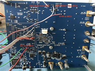
我将 PCM1863的外部 I2S 4线直接连接到散热器和 J9外部板连接器之间的测试点、并可以使用逻辑分析仪正确读取它们。
来自 MCU 的 I2C 直接连接 到 EVM 上的 SCL 和 SDA 测试点。 我使用逻辑分析仪检查了 I2C 数据、所有寄存器似乎都已正确设置。
电路板设置如下:
1) 1)设置 J35 (从模式)
2) 2) J19未设置(地址0x96或0x4B)
3) J3、J4、J6、J7设置为 EXT
4) 4) J9设置为 SDIN
5) 5) J37 I2S 选择未设置(AIB I2S)
6) 6) J22设置为主模式
7) 7) J33未设置(XMOS 禁用)
8) 8)移除了 R54和 R55 (I2C 来自我的 PIC MCU)
9) S1 (DAC 静音)和 S3 (放大器复位)设置为正常、并连接到 MCU 以控制启动序列。
MCLK 为12.29MHz、LRCLK 为48kHz、BCLK 为3.07MHz。
在输出端子上、我可以读取600kHz 开关频率。 我的输入信号是1kHz 正弦波。
我是否遗漏了什么? 请告诉我。
此致 
下面是我 使用的寄存器配置(来自 PPC3)和代码以及启动序列:
cfg_reg registers[] = {
//program memory
    { 0x00, 0x00 },
    { 0x7f, 0x00 },		//Switch to Book 0
    { 0x02, 0x11 },		//PowerDown DSP. Bit 0 not documented
    { 0x01, 0x11 },		//Reset module & registers. Bits are auto cleared
    { 0x00, 0x00 },		//Wait
    { 0x00, 0x00 },
    { 0x00, 0x00 },
    { 0x00, 0x00 },
    { 0x03, 0x11 },		//Mute L&R
    { 0x2a, 0x00 },		//Zero Data path L&R (= mute...)
    { 0x25, 0x18 },		//Ignore MCLK error detection
    { 0x0d, 0x00 },		//Clck config..
    { 0x02, 0x00 },		//Wake up DSP
//Sample rate update
    { 0x00, 0x00 },
    { 0x7f, 0x00 },		//Switch to Book0 ... again
    { 0x02, 0x80 },		//Reset DSP
    { 0x00, 0x00 },
    { 0x7f, 0x00 },		//Switch to Book0 ... again
// speed 03-48k 04-96k
//dynamically reading speed
    { 0x22, 0x03 },		//Set FS Speed. Ignored in auto clock mode
    { 0x00, 0x00 },		//Switch to Book0 ... again
    { 0x7f, 0x00 },
    { 0x02, 0x00 },		//Restart DSP
//write coefficients of various components
    { 0x00, 0x00 },		//Switch to Book8c
    { 0x7f, 0x8c },
    { 0x00, 0x1e },
    { 0x44, 0x00 },		//Vol to 0dB
    { 0x45, 0x80 },
    { 0x46, 0x00 },
    { 0x47, 0x00 },
    { 0x48, 0x00 },
    { 0x49, 0x80 },
    { 0x4a, 0x00 },
    { 0x4b, 0x00 },

//swap command
    { 0x00, 0x00 },
    { 0x7f, 0x8c },		//Switch to Book8c
    { 0x00, 0x23 },		//Goto Page 23
    { 0x14, 0x00 },		//Write 00 00 00 01 in reg 0x14+
    { 0x15, 0x00 },
    { 0x16, 0x00 },
    { 0x17, 0x01 },

//register tuning
    { 0x00, 0x00 },
    { 0x7f, 0x00 },		//Switch to Book0
    { 0x00, 0x00 },
    { 0x07, 0x00 },		//SDOut is post processing output
    { 0x08, 0x20 },		//SDOut is output. No mute from PCM
    { 0x55, 0x16 },		//SDOut mux selector - DSP Boot done
    { 0x00, 0x00 },
    { 0x7f, 0x00 },		//Switch to Book0
    { 0x00, 0x00 },
    { 0x3d, 0x24 },		//Digital volume Left	-18dB
    { 0x3e, 0x24 },		//Digital volume Right
    { 0x00, 0x00 },
    { 0x7f, 0x00 },		//Switch to Book0
    { 0x00, 0x01 },		//Switch to Page1
    { 0x02, 0x00 },		//Analog Gain set to 0dB
    { 0x06, 0x01 },		//Analog mute follows digital mute


//Unmute the device
    { 0x00, 0x00 },		//Switch to Book0
    { 0x7f, 0x00 },
    { 0x03, 0x00 },		//UnMute L&R
    { 0x2a, 0x11 },		//Enable data path (L-L & R-R)

};


void init_registers(cfg_reg *r, int n)
 {
    int i = 0;

    while (i < n) {
        switch (r[i].command) {
        case CFG_META_SWITCH:
            // Used in legacy applications.  Ignored here.
            break;
        case CFG_META_DELAY:
            __delay_ms(r[i].param);
            break;
         case CFG_META_BURST:
             I2C1_Send_PA((unsigned char *)&r[i+1], r[i].param);
            i +=  (r[i].param + 1)/2;
            break;
        default:
            I2C1_Send_PA(r[i].offset, r[i].value);
            break;
        }
        i++;
    }
 }


void PA_startup_sequence()
{
    reset_sequence();

    __delay_ms(50);

    init_registers(registers, sizeof(registers)/sizeof(registers[0]));

    __delay_ms(400);

    //adjust_volume();

    //Enable the amplifier output stage by setting the RESET_AMP pin high.
    PA_RESET_SetHigh();

    // Enable DAC
    PA_DAC_MUTE_SetHigh();

}
void shutdown_sequence()
{
  //code for shutdown_sequence
    PA_RESET_SetLow();
}

//code for fault_sequence
void fault_sequence()
{
  // Wait until system temperature gets back to normal temperature: /CLIP_OTW high
  while (PA_OTW_GetValue() == 0)
  {
    __delay_ms(100);
  }
  PA_RESET_SetLow();
  __delay_ms(10);
  PA_RESET_SetHigh();
}

void reset_sequence()
{
  PA_RESET_SetLow(); // Set Amp reset pin low
  PA_DAC_MUTE_SetLow(); // Set Dac mute pin low
}
