This thread has been locked.

If you have a related question, please click the "Ask a related question" button in the top right corner. The newly created question will be automatically linked to this question.

[参考译文] ADS131E08EVM-PDK:使用 SPI + DMA 的 ADS131E08EVM-PDK 在读取/写入寄存器时获取垃圾数据。

Guru**** 691210 points
Other Parts Discussed in Thread: ADS131E08EVM-PDK, ADS131E08
请注意,本文内容源自机器翻译,可能存在语法或其它翻译错误,仅供参考。如需获取准确内容,请参阅链接中的英语原文或自行翻译。

https://e2e.ti.com/support/data-converters-group/data-converters/f/data-converters-forum/1114046/ads131e08evm-pdk-ads131e08evm-pdk-using-spi-dma-getting-garbage-data-when-read-write-register

器件型号:ADS131E08EVM-PDK
主题中讨论的其他器件: ADS131E08

您好、支持团队、

目前、我正在使用 STM32H745发现板处理 ADS131E08EVM-PDK 开发套件。

情景1.

-使用正常 SPI 发送-接收功能通过 ADS131E08寄存器进行读/写操作。

情形2.

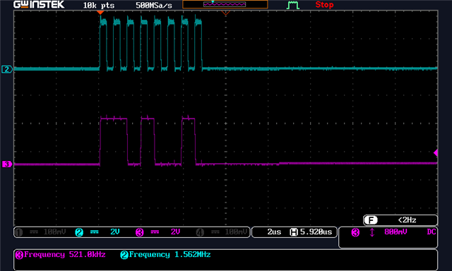
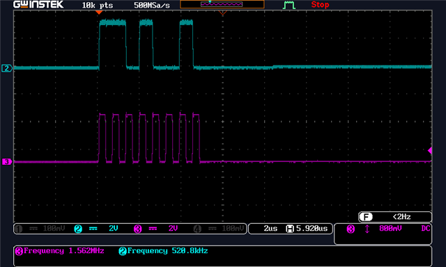
-当我使用  STM32H745发现板为 SPI 配置了 DMA 并为 ADS131E08的读/写寄存器使用 Transmit -Receive_DMA 功能时。

然后得到一些垃圾值。

STM32H745发现板需要任何特定配置?

此 ADS131E08 EVK 的 SPI+DMA 通信可使用任何示例。 对我来说很好。

环境详细信息:

硬件:ADS13xE08EVM Rev A, STM32H745 Discovery 板。

IDE 安装程序:STM32 Cube 版本:1.8.0

  • 请注意,本文内容源自机器翻译,可能存在语法或其它翻译错误,仅供参考。如需获取准确内容,请参阅链接中的英语原文或自行翻译。

    您好、Hardiddh、

    感谢您的发帖、欢迎来到我们的 E2E 论坛!

    我建议使用逻辑分析仪仔细检查 ADS131E08和 STM32H745 Discovery 板之间的 SPI 事务。 这将有助于确认 SPI 帧和信号时序与数据表时序要求相匹配。 当您不使用 DMA 时、器件似乎工作正常、因此我们知道、当您在正常 SPI 模式下降低速度时、数据收集工作正常。

    使用 DMA 时、您是否继续监测来自 ADC 的 DRDYn 中断? 如果您将 SPI 事务与 DRDYn 一起记录、并且您注意到 DRDYn 下降沿出现在 SPI 帧的中间、这将解释数据看起来像垃圾数据的原因。 在每个 DRDYn 下降沿之后、旧数据会立即被新数据覆盖、这会直接传输到输出移位寄存 器并在 DOUT 引脚上读取、即使它发生在活动 SPI 帧的中间也是如此。

    遗憾的是、在发现板上配置 DMA 超出了我们论坛的范围。 您必须将有关发现板的任何问题直接提交给 STMICRO。

    此致、

    Ryan

  • 请注意,本文内容源自机器翻译,可能存在语法或其它翻译错误,仅供参考。如需获取准确内容,请参阅链接中的英语原文或自行翻译。

    您好、Ryan、

    感谢您简要回答我的问题。

    目前、我没有读取任何 ADC 通道数据。 因此、DRDYn 引脚数据的范围目前主要使用 DOUT 和 DIN。

    1:配置 ADS131E08启动序列的读/写寄存器。

    2.同时执行电源启动序列。

    首先发送 ADS131E08_CMD_SDATAC (用于停止连续数据),然后使用 E08_CONFIG1_ADDRESS 读取一个配置寄存器。

    此外、我已在下面共享了我的代码、请查看此代码。

    如果您有 ADS131E08驱动程序代码的任何示例源代码。 请与我分享。

    这对我们非常有帮助。

    注意:我们已使用两个 STM32H745板验证了 SPI+DMA 代码、该代码工作正常。

    //////////////////////////////////////////////ADS131E08/////////////////////////////////////////////////////////////////////
    
    /*
     * Copyright 2021 Minchul Jun (mcjun37@naver.com).  All rights reserved.
     *
     * Redistribution and use in source and binary forms, with or without
     * modification, are permitted provided that the following conditions are met:
     *
     *   1. Redistributions of source code must retain the above copyright notice,
     *      this list of conditions and the following disclaimer.
     *
     *   2. Redistributions in binary form must reproduce the above copyright
     *      notice, this list of conditions and the following disclaimer in the
     *      documentation and/or other materials provided with the distribution.
     *
     * THIS SOFTWARE IS PROVIDED BY MINCHUL JUN ``AS IS'' AND ANY EXPRESS OR IMPLIED
     * WARRANTIES, INCLUDING, BUT NOT LIMITED TO, THE IMPLIED WARRANTIES OF
     * MERCHANTABILITY AND FITNESS FOR A PARTICULAR PURPOSE ARE DISCLAIMED. IN NO
     * EVENT SHALL MINCHUL JUN OR CONTRIBUTORS BE LIABLE FOR ANY DIRECT, INDIRECT,
     * INCIDENTAL, SPECIAL, EXEMPLARY, OR CONSEQUENTIAL DAMAGES (INCLUDING, BUT
     * NOT LIMITED TO, PROCUREMENT OF SUBSTITUTE GOODS OR SERVICES; LOSS OF USE,
     * DATA, OR PROFITS; OR BUSINESS INTERRUPTION) HOWEVER CAUSED AND ON ANY
     * THEORY OF LIABILITY, WHETHER IN CONTRACT, STRICT LIABILITY, OR TORT
     * (INCLUDING NEGLIGENCE OR OTHERWISE) ARISING IN ANY WAY OUT OF THE USE OF
     * THIS SOFTWARE, EVEN IF ADVISED OF THE POSSIBILITY OF SUCH DAMAGE.
     *
     * The views and conclusions contained in the software and documentation are
     * those of the authors and should not be interpreted as representing official
     * policies, either expressed or implied, of Minchul Jun.
     *
     */
    
    #include "ADS131E08.h"
    #include "cmsis_os.h"
    #include "stdlib.h"
    #include "string.h"
    #include "stm32h7xx_it.h"
    #include "spi.h"
    #include "main.h"
    
    _adcConfE* adcConfE0 = NULL;
    _adcConfE* adcConfE1 = NULL;
    
    extern uint32_t failcnt;
    extern uint32_t successcnt;
    //extern uint8_t aTxBuffer[50];
    extern uint8_t aRxBuffer[50];
    enum {
      TRANSFER_WAIT,
      TRANSFER_COMPLETE,
      TRANSFER_ERROR
    };
    extern enum Trnsfer_state state;
    uint32_t TransferStat = TRANSFER_WAIT;
    void ADS131E08_control_start_signal(_signalState onOff);
    void ADS131E08_control_reset_signal(_signalState onOff);
    void ADS131E08_control_cs_signal(_adcType adcType, _signalState onOff);
    GPIO_PinState ADS131E08_read_cs_signal(_adcType adcType);
    HAL_StatusTypeDef ADS131E08_startup(_adcType adcType);
    HAL_StatusTypeDef ADS131E08_send_command(_adcConfE* adcConfE, uint16_t cmd, uint16_t addr, uint8_t regs, uint16_t regNo);
    void ADS131E08_set_default_register(_adcConfE* adcConfE);
    
    void ADS131E08_init(_adcType adcType, SPI_HandleTypeDef* hspi)
    {
    
        if(adcType == ADS131E08_ADC20)
        {
            adcConfE0                  = (_adcConfE*)malloc(sizeof(_adcConfE));
            memset(adcConfE0, 0, sizeof(_adcConfE));
            adcConfE0->type            = adcType;
            adcConfE0->stat            = ADS131E08_INIT;
            adcConfE0->hspi            = hspi;
            adcConfE0->nReset.port     = SPI1_NRESET_GPIO_Port;
            adcConfE0->nReset.pin      = SPI1_NRESET_Pin;
            adcConfE0->cs.port         = SPI1_CS0_GPIO_Port;
            adcConfE0->cs.pin          = SPI1_CS0_Pin;
            adcConfE0->nDrdy.port      = SPI1_INT_GPIO_Port;
            adcConfE0->nDrdy.pin       = SPI1_INT_Pin;
            adcConfE0->start.port      = SPI1_START_GPIO_Port;
            adcConfE0->start.pin       = SPI1_START_Pin;
            adcConfE0->bufLen          = E08_WORDS_IN_FRAME * E08_WORD_LENGTH + 1;      // 9 Words x 24 Bits = 216 Bits (27 Bytes) + 1 (command byte)
            adcConfE0->rxBuf           = (uint8_t*)malloc(adcConfE0->bufLen);
            memset(adcConfE0->rxBuf, 0, adcConfE0->bufLen);
            adcConfE0->txBuf           = (uint8_t*)malloc(adcConfE0->bufLen);
    
            ADS131E08_set_default_register(adcConfE0);
        }
    //    else if(adcType == ADS131E08_ADC21)
    //    {
    //        adcConfE1                  = (_adcConfE*)malloc(sizeof(_adcConfE));
    //        memset(adcConfE1, 0, sizeof(_adcConfE));
    //        adcConfE1->type            = adcType;
    //        adcConfE1->stat            = ADS131E08_INIT;
    //        adcConfE1->hspi            = hspi;
    //        adcConfE1->nReset.port     = SPI1_NRESET_GPIO_Port;
    //        adcConfE1->nReset.pin      = SPI1_NRESET_Pin;
    //        adcConfE1->cs.port         = SPI1_CS1_GPIO_Port;
    //        adcConfE1->cs.pin          = SPI1_CS1_Pin;
    //        adcConfE1->nDrdy.port      = SPI1_INT_GPIO_Port;
    //        adcConfE1->nDrdy.pin       = SPI1_INT_Pin;
    //        adcConfE1->start.port      = SPI1_START_GPIO_Port;
    //        adcConfE1->start.pin       = SPI1_START_Pin;
    //        adcConfE1->bufLen          = E08_WORDS_IN_FRAME * E08_WORD_LENGTH;      // 9 Words x 24 Bits
    //        adcConfE1->rxBuf           = (uint8_t*)malloc(adcConfE1->bufLen);
    //        memset(adcConfE1->rxBuf, 0, adcConfE1->bufLen);
    //        adcConfE1->txBuf           = (uint8_t*)malloc(adcConfE1->bufLen);
    //
    //        ADS131E08_set_default_register(adcConfE1);
    //    }
        else
        {
            // DO NOTHING
        }
    
        return;
    }
    
    SPI_HandleTypeDef* ADS131E08_is_spi_type(_adcType adcType)
    {
        if(adcType == ADS131E08_ADC20)
        {
            return adcConfE0->hspi;
        }
        else if(adcType == ADS131E08_ADC21)
        {
            return adcConfE1->hspi;
        }      
        else
        {
            return NULL;
        }
    }
    
    uint8_t* ADS131E08_is_rxbuf(_adcType adcType)
    {
        if(adcType == ADS131E08_ADC20)
        {
            return adcConfE0->rxBuf;
        }
        else if(adcType == ADS131E08_ADC21)
        {
            return adcConfE1->rxBuf;
        }     
        else
        {
            return NULL;
        }
    }
    
    _ADS131E08_stat ADS131E08_is_adc_status(_adcType adcType)
    {
        if(adcType == ADS131E08_ADC20)
        {
            return adcConfE0->stat;
        }
        else if(adcType == ADS131E08_ADC21)
        {
            return adcConfE1->stat;
        }    
        else
        {
            return 0;
        }
    }
    
    void ADS131E08_set_adc_status(_adcType adcType, _ADS131E08_stat stat)
    {
        if(adcType == ADS131E08_ADC20)
        {
            adcConfE0->stat  = stat;
        }
        else if(adcType == ADS131E08_ADC21)
        {
            adcConfE1->stat = stat;
        }
        else
        {
            // DO NOTHING
        }
        return;
    }
    
    uint8_t ADS131E08_is_buf_len(_adcType adcType)
    {
        if(adcType == ADS131E08_ADC20)
        {
            return adcConfE1->bufLen;
        }
        else if(adcType == ADS131E08_ADC21)
        {
            return adcConfE1->bufLen;
        }        
        else
        {
            return 0;
        }
    }
    
    HAL_StatusTypeDef ADS131E08_send_command(_adcConfE* adcConfE, uint16_t cmd, uint16_t addr, uint8_t regs, uint16_t regNo)
    {
        const uint16_t cmdLen = 2;        // Command byte length (2 Bytes)
        HAL_StatusTypeDef result = HAL_OK;
    
        memset(adcConfE->txBuf, 0, adcConfE->bufLen);
        switch(cmd)
        {
            case ADS131E08_CMD_WAKEUP:
            case ADS131E08_CMD_STANDBY:
            case ADS131E08_CMD_RESET:
            case ADS131E08_CMD_RDATAC:
            case ADS131E08_CMD_SDATAC:
            case ADS131E08_CMD_RDATA:
                adcConfE->txBuf[0] = ADS131E08_UPPER(cmd);
                adcConfE->txBuf[1] = ADS131E08_LOWER(cmd);
                adcConfE->txBuf[2] = 0;
                adcConfE->txBuf[3] = 0;
                adcConfE->command = cmd;
                adcConfE->regAddr = 0;
                break;
            case ADS131E08_CMD_RREG:    // ADS131E08_CMD_RREGS
                adcConfE->txBuf[0] = ADS131E08_UPPER(ADS131E08_REG_COMMAND(cmd,addr,regNo));
                adcConfE->txBuf[1] = ADS131E08_LOWER(ADS131E08_REG_COMMAND(cmd,addr,regNo));
                adcConfE->txBuf[2] = 0;
                adcConfE->txBuf[3] = 0;
                adcConfE->command = cmd;
                adcConfE->regAddr = addr;
                adcConfE->regs = regs;
                break;
            case ADS131E08_CMD_WREG:
                adcConfE->txBuf[0] = ADS131E08_UPPER(ADS131E08_REG_COMMAND(cmd,addr,regNo));
                adcConfE->txBuf[1] = ADS131E08_LOWER(ADS131E08_REG_COMMAND(cmd,addr,regNo));
                adcConfE->txBuf[2] = ADS131E08_UPPER(ADS131E08_REG_REGDATA(regs));
                adcConfE->txBuf[3] = ADS131E08_LOWER(ADS131E08_REG_REGDATA(regs));
                adcConfE->command = cmd;
                adcConfE->regAddr = addr;
                adcConfE->regs = regs;
                break;
            default:
                break;
        }
    
        // Wait until cs pin is reset to send data
        while(GPIO_PIN_RESET == ADS131E08_read_cs_signal(adcConfE->type))
        {}
    
        ADS131E08_control_cs_signal(adcConfE->type, RESET_SIGNAL);
        if(cmd == ADS131E08_CMD_RREG)        
        {
            result = HAL_SPI_TransmitReceive(adcConfE->hspi, adcConfE->txBuf, adcConfE->rxBuf, cmdLen, 10);
            memset(adcConfE->rxBuf, 0, adcConfE->bufLen);
            result = HAL_SPI_Receive(adcConfE->hspi, adcConfE->rxBuf, regNo, 500);        
    
            // Update Register Status
            adcConfE->sr.mp[adcConfE->regAddr] = adcConfE->rxBuf[0];
        }
        else if(cmd == ADS131E08_CMD_WREG)
        {
            result = HAL_SPI_TransmitReceive(adcConfE->hspi, adcConfE->txBuf, adcConfE->rxBuf, regNo + cmdLen, 10);
        }
        else if(cmd == ADS131E08_CMD_RDATA)
        {
            memset(adcConfE->rxBuf, 0, adcConfE->bufLen);
            result = HAL_SPI_TransmitReceive(adcConfE->hspi, adcConfE->txBuf, adcConfE->rxBuf, 28, 10);
        }
        else
        {
            result = HAL_SPI_TransmitReceive(adcConfE->hspi, adcConfE->txBuf, adcConfE->rxBuf, cmdLen, 10);
        }
        ADS131E08_control_cs_signal(adcConfE->type, SET_SIGNAL);
    
        return result;
    }
    
    uint32_t ADS131E08_convert_adc_data(const uint8_t* dataBuf)
    {
        uint32_t upperByte = 0;
        uint32_t middleByte = 0;
        uint32_t lowerByte = 0;
    
        // The output data extends to 32 bits with eight zeroes(0b00000000, 1Byte) added to the least significant bits when using the 32-bit device word length setting, datasheet 38p
        upperByte    = ((uint32_t)(dataBuf[0] << 16) & 0x00FF0000);
        middleByte   = ((uint32_t)(dataBuf[1] << 8) & 0x0000FF00);
        lowerByte    = ((uint32_t)(dataBuf[2] << 0) & 0x000000FF);
    
        return (upperByte | middleByte | lowerByte);
    }
    
    float ADS131E08_convert_to_mVolt(uint32_t reg)
    {
        const float unitFS = 5000.0f / 8388607.0f; // unit: mV (if unit is V, calculated value is out of 'float' range)
        const uint32_t boundaryValue = 0x7FFFFF; // threshold of positive value
        int signFlg = 0;        // +: 1, -: -1
    
        // negative value
        if (reg > boundaryValue)
        {
            reg = (0xFFFFFF - reg) + 1; // if value is 0xFFFFFF, register is -FS/2^23. so plus 1
            signFlg = -1;
        }
        // positive value
        else
        {
            signFlg = 1;
        }
    
        // convert register to mVolt
        return (unitFS * (float)reg * (float)signFlg);
    }
    
    void ADS131E08_parse_adc_data(_adcType adcType)
    {
        _ADS131E08_ch ch;
        uint8_t index;
        uint32_t temp;
        uint32_t sTemp;
        const uint8_t preBitCode = 0b1100;
        uint8_t recvPreBitCode;
        _adcConfE* adcConfE;
        uint8_t* buf;
    
        if(adcType == ADS131E08_ADC20)
        {
            adcConfE = adcConfE0;
        }
        else if(adcType == ADS131E08_ADC21)
        {
            adcConfE = adcConfE1;
        }
        else
        {
            // DO NOTHING
            return;
        }
    
        // Reading Back Packet
        // 24 Status Bits + 24 Bits per channel x 8 channels = 216 bits
    
        /* Status Word Content (24 bits)
        * ---------------------------------------------------------------------------------------------------------------------
        * | Bit 23 | Bit 22 | Bit 21 | Bit 20 | Bit 19 |  ....  | Bit 12 | Bit 11 |  ....  | Bit 04 | Bit 03 |  .... | Bit 00 |
        * ---------------------------------------------------------------------------------------------------------------------
        * |    1   |    1   |    0   |    0   |     FAULT_STATP[7:0]     |     FAULT_STATN[7:0]     |        GPIO[7:4]        |
        * ---------------------------------------------------------------------------------------------------------------------
        */
    
        // rxBuf[0] is response for command(RDATA), so status buf start at rxBuf[1]
        temp = ADS131E08_MERGE_BYTE(adcConfE->rxBuf[1], adcConfE->rxBuf[2], adcConfE->rxBuf[3]);
    
        recvPreBitCode = (uint8_t)((temp & 0x00F00000) >> 20);
    
        if(recvPreBitCode != preBitCode)
        {
            // DO NOTHING
        }
    
        // Shift 4 bits to remove pre bit code(0b1100)
        sTemp = temp << 4;
        // Update Status Register
        adcConfE->sr.mp[E08_FAULT_STATP_ADDRESS]    = ADS131E08_FETCH_UPPER(sTemp);
        adcConfE->sr.mp[E08_FAULT_STATN_ADDRESS]    = ADS131E08_FETCH_MIDDLE(sTemp);
        adcConfE->sr.mp[E08_GPIO_ADDRESS]           = ADS131E08_FETCH_LOWER(sTemp) & 0xF0;
    
        // data buf start at rxBuf[4]
        buf = &adcConfE->rxBuf[4];
    
        for(ch = ADC_CH1, index = 0; ch < NUMB_ADC_CH; ch++, index++)
        {
            adcConfE->chData[ch].r = ADS131E08_convert_adc_data(&buf[index * E08_WORD_LENGTH]);        
            adcConfE->chData[ch].v = ADS131E08_convert_to_mVolt(adcConfE->chData[ch].r);
        }
    }
    // ADC1 and ADC2 share a start signal.
    // Start signal is related to generate /DRDY signal
    void ADS131E08_control_start_signal(_signalState onOff)
    {
        if(onOff == SET_SIGNAL)
        {
           HAL_GPIO_WritePin(adcConfE0->start.port, adcConfE0->start.pin, GPIO_PIN_SET);
        }
        else if(onOff == RESET_SIGNAL)
        {
            HAL_GPIO_WritePin(adcConfE0->start.port, adcConfE0->start.pin, GPIO_PIN_RESET);
        }
        else
        {
            // Do Nothing
        }
    }
    
    void ADS131E08_receive_data(_adcType adcType)
    {
        _adcConfE* adcConfE = NULL;
        if(adcType == ADS131E08_ADC20)
        {
            adcConfE = adcConfE0;
        }
        else if(adcType == ADS131E08_ADC21)
        {
            adcConfE = adcConfE1;
        }
        else
        {
            // DO NOTHING
            return;
        }
    
        // Wait until cs pin is reset to send data
        while(GPIO_PIN_RESET == ADS131E08_read_cs_signal(adcConfE->type))
        {}
        ADS131E08_control_cs_signal(adcConfE->type, RESET_SIGNAL);
        HAL_SPI_Receive(adcConfE->hspi, adcConfE->rxBuf, adcConfE->bufLen, 50);
        ADS131E08_control_cs_signal(adcConfE->type, SET_SIGNAL);
    }
    
    // RDATA command is related to conversion data
    void ADS131E08_send_rdatac_cmd()
    {
        ADS131E08_send_command(adcConfE0, ADS131E08_CMD_RDATAC, 0, 0, 1);
        ADS131E08_send_command(adcConfE1, ADS131E08_CMD_RDATAC, 0, 0, 1);
    }
    
    // RDATA command is related to conversion data
    void ADS131E08_send_rdata_cmd(_adcType adcType)
    {
        if(adcType == ADS131E08_ADC20)
        {
            ADS131E08_send_command(adcConfE0, ADS131E08_CMD_RDATA, 0, 0, 1);
        }
        else if(adcType == ADS131E08_ADC21)
        {
            ADS131E08_send_command(adcConfE1, ADS131E08_CMD_RDATA, 0, 0, 1);
        }
    }
    
    
    void ADS131E08_control_reset_signal(_signalState onOff)
    {
        if(onOff == SET_SIGNAL)
        {
           HAL_GPIO_WritePin(adcConfE0->nReset.port, adcConfE0->nReset.pin, GPIO_PIN_SET);
        }
        else if(onOff == RESET_SIGNAL)
        {
            HAL_GPIO_WritePin(adcConfE0->nReset.port, adcConfE0->nReset.pin, GPIO_PIN_RESET);
        }
        else
        {
            // Do Nothing
        }
    }
    
    void ADS131E08_control_cs_signal(_adcType adcType, _signalState onOff)
    {
        if(onOff == SET_SIGNAL)
        {
            if(adcType == ADS131E08_ADC20)
            {
                HAL_GPIO_WritePin(adcConfE0->cs.port, adcConfE0->cs.pin, GPIO_PIN_SET);
            }
            else if(adcType == ADS131E08_ADC21)
            {
                HAL_GPIO_WritePin(adcConfE1->cs.port, adcConfE1->cs.pin, GPIO_PIN_SET);
            }
            else
            {
                // DO NOTHING
            }
    
        }
        else if(onOff == RESET_SIGNAL)
        {
            if(adcType == ADS131E08_ADC20)
            {
                HAL_GPIO_WritePin(adcConfE0->cs.port, adcConfE0->cs.pin, GPIO_PIN_RESET);
            }
            else if(adcType == ADS131E08_ADC21)
            {
                HAL_GPIO_WritePin(adcConfE1->cs.port, adcConfE1->cs.pin, GPIO_PIN_RESET);
            }
            else
            {
                // DO NOTHING
            }
        }
        else
        {
            // Do Nothing
        }
    }
    
    GPIO_PinState ADS131E08_read_cs_signal(_adcType adcType)
    {
        if(adcType == ADS131E08_ADC20)
        {
            return HAL_GPIO_ReadPin(adcConfE0->cs.port, adcConfE0->cs.pin);
        }
        else if(adcType == ADS131E08_ADC21)
        {
            return HAL_GPIO_ReadPin(adcConfE1->cs.port, adcConfE1->cs.pin);
        }
    
        return 0;
    }
    
    void ADS131E08_set_default_register(_adcConfE* adcConfE)
    {
        adcConfE->sr.mp[E08_ID_ADDRESS]              =   0x00;                                  /* NOTE: This a read-only register */
        adcConfE->sr.mp[E08_CONFIG1_ADDRESS]         =   E08_CONFIG1_DEFAULT;                   /* NOTE: REV_ID value is unknown until read */
        adcConfE->sr.mp[E08_CONFIG2_ADDRESS]         =   E08_CONFIG2_DEFAULT;
        adcConfE->sr.mp[E08_CONFIG3_ADDRESS]         =   E08_CONFIG3_DEFAULT;
        adcConfE->sr.mp[E08_FAULT_ADDRESS]           =   E08_FAULT_DEFAULT;
        adcConfE->sr.mp[E08_CH1SET_ADDRESS]          =   E08_CH1SET_DEFAULT;
        adcConfE->sr.mp[E08_CH2SET_ADDRESS]          =   E08_CH2SET_DEFAULT;
        adcConfE->sr.mp[E08_CH3SET_ADDRESS]          =   E08_CH3SET_DEFAULT;
        adcConfE->sr.mp[E08_CH4SET_ADDRESS]          =   E08_CH4SET_DEFAULT;
        adcConfE->sr.mp[E08_CH5SET_ADDRESS]          =   E08_CH5SET_DEFAULT;
        adcConfE->sr.mp[E08_CH6SET_ADDRESS]          =   E08_CH6SET_DEFAULT;
        adcConfE->sr.mp[E08_CH7SET_ADDRESS]          =   E08_CH7SET_DEFAULT;
        adcConfE->sr.mp[E08_CH8SET_ADDRESS]          =   E08_CH8SET_DEFAULT;
        adcConfE->sr.mp[E08_FAULT_STATP_ADDRESS]     =   E08_FAULT_STATP_DEFAULT;
        adcConfE->sr.mp[E08_FAULT_STATN_ADDRESS]     =   E08_FAULT_STATN_DEFAULT;
        adcConfE->sr.mp[E08_GPIO_ADDRESS]            =   E08_GPIO_DEFAULT;
    }
    
    void ADS131E08_initial_flow_at_power_up(_adcConfE* adcConfE)
    {
        int i;
        volatile uint8_t regs, addr;
    
        // Always send a SDATAC command first to stop continuous conversion and write register.
        ADS131E08_send_command(adcConfE, ADS131E08_CMD_SDATAC, 0, 0, 1);
    
        ///////////////////////////////////////
        // Read ID Register
        ///////////////////////////////////////
        ADS131E08_send_command(adcConfE, ADS131E08_CMD_RREG, E08_ID_ADDRESS, 0, 1);
    
        ///////////////////////////////////////
        // Write Configuration 1 Register
        ///////////////////////////////////////
        // Set register with default
        regs = E08_CONFIG1_DEFAULT;
    
        ADS131E08_send_command(adcConfE, ADS131E08_CMD_WREG, E08_CONFIG1_ADDRESS, regs, 2);
        // Confirm whether written or not.
        ADS131E08_send_command(adcConfE, ADS131E08_CMD_RREG, E08_CONFIG1_ADDRESS, 0, 1);
    
    
        ///////////////////////////////////////
        // Write Configuration 2 Register
        ///////////////////////////////////////
        // Set register with default
        regs = E08_CONFIG2_DEFAULT;
    
        ADS131E08_send_command(adcConfE, ADS131E08_CMD_WREG, E08_CONFIG2_ADDRESS, regs, 2);
        // Confirm whether written or not.
        ADS131E08_send_command(adcConfE, ADS131E08_CMD_RREG, E08_CONFIG2_ADDRESS, 0, 1);
    
        ///////////////////////////////////////
        // Write CHnSET Register
        ///////////////////////////////////////
        // Set input short to middle voltage (Input shorted to (AVDD + AVSS) / 2 (for offset or noisemeasurements))
        regs = E08_CH1SET_MUX_MASK & E08_CH1SET_MUX_INPUT_SHORT_TO_MID;
        addr = E08_CH1SET_ADDRESS;
        for(i = 0; i < NUMB_ADC_CH; i++, addr++)
        {
            ADS131E08_send_command(adcConfE, ADS131E08_CMD_WREG, addr, regs, 2);
            // Confirm whether written or not.
            ADS131E08_send_command(adcConfE, ADS131E08_CMD_RREG, addr, 0, 1);
        }
        // Activate Conversion
        ADS131E08_control_start_signal(SET_SIGNAL);
    
        // Send RDATAC command
        ADS131E08_send_command(adcConfE, ADS131E08_CMD_RDATAC, 0, 0, 1);
    
        // Capture Data and Check Noise
        // Look for /DRDY and Issue 24 + n x 24 SCLKs
        for(i = 0; i < 1; i++)
        {
            //ADS131E08_wait_drdy_int(100);
            HAL_Delay(100);
            ADS131E08_control_cs_signal(adcConfE->type, RESET_SIGNAL);
            HAL_SPI_Receive(adcConfE->hspi, adcConfE->rxBuf, adcConfE->bufLen, 500);
            ADS131E08_control_cs_signal(adcConfE->type, SET_SIGNAL);
        }
    
        // Always send a SDATAC command first to stop continuous conversion and write register.
        ADS131E08_send_command(adcConfE, ADS131E08_CMD_SDATAC, 0, 0, 1);
    
        ///////////////////////////////////////
        // Write Configuration 2 Register
        ///////////////////////////////////////
        // Set that test signal are generated internally (Activate a (1mV / 2.4V) Square-Wave Test Signal)
        regs = E08_CONFIG2_INT_TEST_MASK & E08_CONFIG2_INT_TEST_ENABLE;
    
        ADS131E08_send_command(adcConfE, ADS131E08_CMD_WREG, E08_CONFIG2_ADDRESS, regs, 2);
        // Confirm whether written or not.
        ADS131E08_send_command(adcConfE, ADS131E08_CMD_RREG, E08_CONFIG2_ADDRESS, 0, 1);
    
        ///////////////////////////////////////
        // Write CHnSET Register
        ///////////////////////////////////////
        // Set test signal enable on All Channels
        regs = E08_CH1SET_MUX_MASK & E08_CH1SET_MUX_TEST_SIGNAL;
        addr = E08_CH1SET_ADDRESS;
        for(i = 0; i < NUMB_ADC_CH; i++, addr++)
        {
            ADS131E08_send_command(adcConfE, ADS131E08_CMD_WREG, addr, regs, 2);
            // Confirm whether written or not.
            ADS131E08_send_command(adcConfE, ADS131E08_CMD_RREG, addr, 0, 1);
        }
    
        // Send RDATAC command
        ADS131E08_send_command(adcConfE, ADS131E08_CMD_RDATAC, 0, 0, 1);
    
        // Capture Data and Test Signal
        // Look for /DRDY and Issue 24 + n x 24 SCLKs
        for(i = 0; i < 1; i++)
        {
            //ADS131E08_wait_drdy_int(100);
            HAL_Delay(100);
            ADS131E08_control_cs_signal(adcConfE->type, RESET_SIGNAL);
            HAL_SPI_Receive(adcConfE->hspi, adcConfE->rxBuf, adcConfE->bufLen, 500);
            ADS131E08_control_cs_signal(adcConfE->type, SET_SIGNAL);
        }
    
        // Always send a SDATAC command first to stop continuous conversion and write register.
        ADS131E08_send_command(adcConfE, ADS131E08_CMD_SDATAC, 0, 0, 1);
    
        // Stop Conversion
        ADS131E08_control_start_signal(RESET_SIGNAL);    
    }
    
    HAL_StatusTypeDef ADS131E08_startup(_adcType adcType)
    {
        int i;
        volatile uint8_t addr;
        volatile uint8_t regs;
        _adcConfE* adcConfE;
        uint8_t cmdLen;
        cmdLen=4;
        uint16_t cmd;
        uint16_t regNo;
    
    
        if(adcType == ADS131E08_ADC20)
        {
            adcConfE = adcConfE0;
        }
        else if(adcType == ADS131E08_ADC21)
        {
            adcConfE = adcConfE1;
        }
        else
        {
            // DO NOTHING
            return HAL_ERROR;
        }
    
        HAL_Delay(5);
    
        regs = 0;
        cmd = ADS131E08_CMD_SDATAC;
        addr = 0;
        regNo = 1;
        printf("sendding Register write command data over SPI\n");
        adcConfE->txBuf[0] = ADS131E08_UPPER(cmd);
        adcConfE->txBuf[1] = ADS131E08_LOWER(cmd);
        adcConfE->txBuf[2] = 0;
        adcConfE->txBuf[3] = 0;
        adcConfE->command = cmd;
        adcConfE->regAddr = 0;
        TransferStat = TRANSFER_WAIT;
        if(HAL_SPI_TransmitReceive_DMA(&hspi2, adcConfE->txBuf, adcConfE->rxBuf, cmdLen) != HAL_OK)
        {
          /* Transfer error in transmission process */
          Error_Handler();
          printf("HAL_SPI_TrasmitReceive Error \n");
        }
          printf("Data sent waiting for tx satus\n\n");
        while (TransferStat == TRANSFER_WAIT)
        {
    
        }
        printf("Write Command Transfer Completed checking the case\n");
    
    
          //////////////////////////////Test SPI_DMA command with ADS131E08///////////////////////
          regs = E08_CONFIG1_DEFAULT;
          cmd = ADS131E08_CMD_WREG;
          addr = E08_CONFIG1_ADDRESS;
          regNo = 2;
          while (1)
          {
    
              printf("sendding Register write command data over SPI\n");
              adcConfE->txBuf[0] = ADS131E08_UPPER(ADS131E08_REG_COMMAND(cmd,addr,regNo));
              adcConfE->txBuf[1] = ADS131E08_LOWER(ADS131E08_REG_COMMAND(cmd,addr,regNo));
              adcConfE->txBuf[2] = ADS131E08_UPPER(ADS131E08_REG_REGDATA(regs));
              adcConfE->txBuf[3] = ADS131E08_LOWER(ADS131E08_REG_REGDATA(regs));
              adcConfE->command = cmd;
              adcConfE->regAddr = addr;
              adcConfE->regs = regs;
          if(HAL_SPI_TransmitReceive_DMA(&hspi2, adcConfE->txBuf, adcConfE->rxBuf, cmdLen) != HAL_OK)
           {
             /* Transfer error in transmission process */
             Error_Handler();
             printf("HAL_SPI_TrasmitReceive Error \n");
           }
              printf("Data sent waiting for tx satus\n\n");
           while (TransferStat == TRANSFER_WAIT)
           {
           }
            printf("Write Command Transfer Completed checking the case\n");
    
           /* Invalidate cache prior to access by CPU */
           SCB_InvalidateDCache_by_Addr ((uint32_t *)aRxBuffer, BUFFERSIZE);
    
           switch(TransferStat)
           {
             case TRANSFER_COMPLETE :
                 printf("Enter in TX complete case\n");
           /*##-4- Compare the sent and received buffers ##############################*/
               break;
             default :
                 printf("enter in deafult case\n");
               //Error_Handler();
               break;
           }
           HAL_Delay(1000);
    
           ADS131E08_send_command(adcConfE, ADS131E08_CMD_RREG, E08_CONFIG1_ADDRESS, 0, 1);
           printf("sendding Register Read command data over SPI\n");
           adcConfE->txBuf[0] = ADS131E08_UPPER(ADS131E08_REG_COMMAND(cmd,addr,regNo));
           adcConfE->txBuf[1] = ADS131E08_LOWER(ADS131E08_REG_COMMAND(cmd,addr,regNo));
           adcConfE->txBuf[2] = 0;
           adcConfE->txBuf[3] = 0;
           adcConfE->command = cmd;
           adcConfE->regAddr = addr;
           adcConfE->regs = regs;
           regs = E08_CONFIG1_DEFAULT;
           cmd = ADS131E08_CMD_RREG;
           addr = E08_CONFIG1_ADDRESS;
           regNo = 1;
           TransferStat = TRANSFER_WAIT;
           if(HAL_SPI_TransmitReceive_DMA(&hspi2, adcConfE->txBuf, adcConfE->rxBuf, cmdLen) != HAL_OK)
                  {
                    /* Transfer error in transmission process */
                    Error_Handler();
                    printf("HAL_SPI_TrasmitReceive Error \n");
                  }
                     printf("Data sent waiting for tx satus\n\n");
                  while (TransferStat == TRANSFER_WAIT)
                  {
                  }
                  printf("Read Command Transfer Completed checking the case\n");
    
                  /* Invalidate cache prior to access by CPU */
                  SCB_InvalidateDCache_by_Addr ((uint32_t *)aRxBuffer, BUFFERSIZE);
    
                  switch(TransferStat)
                  {
                    case TRANSFER_COMPLETE :
                        printf("Enter in TX complete case\n");
                  /*##-4- Compare the sent and received buffers ##############################*/
                      break;
                    default :
                        printf("enter in deafult case\n");
                      //Error_Handler();
                      break;
                  }
               TransferStat = TRANSFER_WAIT;
               if(HAL_SPI_TransmitReceive_DMA(&hspi2, adcConfE->txBuf,adcConfE->rxBuf, cmdLen) != HAL_OK)
                      {
                        /* Transfer error in transmission process */
                        Error_Handler();
                        printf("HAL_SPI_TrasmitReceive Error \n");
                      }
               while (TransferStat == TRANSFER_WAIT)
               {
               }
               printf("Register Read successfully  Completed checking the case\n");
               // Update Register Status
               adcConfE->sr.mp[adcConfE->regAddr] = adcConfE->rxBuf[0];
    
        }


        ADS131E08_initial_flow_at_power_up(adcConfE);
    
    //After this power starts we could send the Read/write command.
    
        // Always send an SDATAC command first to stop continuous conversion and write register.
        ADS131E08_send_command(adcConfE, ADS131E08_CMD_SDATAC, 0, 0, 1);
    
        ///////////////////////////////////////
        // Write Configuration 1 Register
        ///////////////////////////////////////
        // Remove register value related with data rate
        regs = E08_CONFIG1_DEFAULT & (~E08_CONFIG1_DR_MASK);
        // Set Data rate to 1 kSPS
        regs |= E08_CONFIG1_DR_MASK & E08_DR_1KSPS;
    
        ADS131E08_send_command(adcConfE, ADS131E08_CMD_WREG, E08_CONFIG1_ADDRESS, regs, 2);
        // Confirm whether written or not.
        HAL_Delay(5);
        ADS131E08_send_command(adcConfE, ADS131E08_CMD_RREG, E08_CONFIG1_ADDRESS, 0, 1);
    
        if(adcConfE->sr.mp[E08_CONFIG1_ADDRESS] != regs)
        {
            return HAL_ERROR;
        }
        else
        {
            // DO NOTHING, Keep going
        }
    
        ///////////////////////////////////////
        // Write Configuration 2 Register
        ///////////////////////////////////////
        // Set register with default
        regs = E08_CONFIG2_DEFAULT;
    
        ADS131E08_send_command(adcConfE, ADS131E08_CMD_WREG, E08_CONFIG2_ADDRESS, regs, 2);
        // Confirm whether written or not.
        ADS131E08_send_command(adcConfE, ADS131E08_CMD_RREG, E08_CONFIG2_ADDRESS, 0, 1);
    
        if(adcConfE->sr.mp[E08_CONFIG2_ADDRESS] != regs)
        {
            return HAL_ERROR;
        }
        else
        {
            // DO NOTHING, Keep going
        }
    
        ///////////////////////////////////////
        // Write CHnSET Register
        ///////////////////////////////////////
        // Set register with default
        regs = E08_CH1SET_DEFAULT;
        addr = E08_CH1SET_ADDRESS;
        for(i = 0; i < NUMB_ADC_CH; i++, addr++)
        {
            ADS131E08_send_command(adcConfE, ADS131E08_CMD_WREG, addr, regs, 2);
            // Confirm whether written or not.
            ADS131E08_send_command(adcConfE, ADS131E08_CMD_RREG, addr, 0, 1);
    
            if(adcConfE->sr.mp[addr] != regs)
            {
                return HAL_ERROR;
            }
            else
            {
                // DO NOTHING, Keep going
            }        
        }
    
        ADS131E08_set_adc_status(adcConfE->type, ADS131E08_NORMAL);
    
        return HAL_OK;
    }
    
    void ADS131E08_send_rdatac_command()
    {
        // Send RDATAC command to ADC20, ADC21 simultaneously.
        ADS131E08_send_command(adcConfE0, ADS131E08_CMD_RDATAC, 0, 0, 1);
        ADS131E08_send_command(adcConfE1, ADS131E08_CMD_RDATAC, 0, 0, 1);
    }
    
    void ADS131E08_initialize_signal()
    {
        // Generate Reset Pulse
        ADS131E08_control_reset_signal(SET_SIGNAL);
        ADS131E08_control_start_signal(RESET_SIGNAL);
        ADS131E08_control_reset_signal(RESET_SIGNAL);
        HAL_Delay(5);
        ADS131E08_control_reset_signal(SET_SIGNAL);
        // Initialize Chip Select signal
        ADS131E08_control_cs_signal(ADS131E08_ADC20, SET_SIGNAL);
        //ADS131E08_control_cs_signal(ADS131E08_ADC21, SET_SIGNAL);
    }
    
    //////////////////////////////////END//////////////////////////////////////////////////////////////////////////////////////////////////////

  • 请注意,本文内容源自机器翻译,可能存在语法或其它翻译错误,仅供参考。如需获取准确内容,请参阅链接中的英语原文或自行翻译。

    您好、Harsiddh、

    然后、可以共享 SPI 通信的逻辑分析仪捕获(即 CSn、SCLK、DIN 和 DOUT)? 了解"垃圾"寄存器数据的含义会有所帮助。

    关于电源定序、我们只建议主机控制器在 AVDD 和 DVDD 电源电压斜升后复位 ADC。 这可以通过 RESET SPI 命令或 RESETn 引脚来实现。 这将确保在启动时正确读取内部编程的位设置、并将器件置于已知的良好运行状态。  

    我们目前无法支持代码审查。 不过、我可以向您介绍我们的 ADS131E08EVM-PDK 软件、其中包括用于 DSP 控制器的固件。 如果这有助于您的开发、欢迎您参考。

    您可以在此处下载 EVM 软件:

    https://www.ti.com/tool/ADS131E08EVM-PDK#order-start-development

    此致、

    Ryan

  • 请注意,本文内容源自机器翻译,可能存在语法或其它翻译错误,仅供参考。如需获取准确内容,请参阅链接中的英语原文或自行翻译。

    您好 Reyan

    感谢您对我的回复给出满意的回答。

    -->然后,是否可以共享 SPI 通信的逻辑分析仪捕捉?

    1) 1)我已连接 DSO 捕获的所有波形。
    -与 ADS131E08EVM-PDK 进行正常 SPI 通信
    -具有 SPI + DMA、可实现与 ADS131E08EVM-PDK 的通信。


    场景1:用于两端进行正常 SPI 配置通信。
             - STM32H745发现,发送经 DSO 输出验证的实际数据。
           -还接收来自 ADS131E08EVM-PDK 的数据、该数据也通过 DSO 输出进行了验证。
           
           
    场景2:对于 ADS131E08EVM-PDK 的 SPI+DMA 配置。
             -通过 DSO 输出验证的 STM32H745侧正确发送数据。
           -成功接收与 SPI+DMA 相同的数据。
          

    SPI+DMA 获取垃圾数据问题已解决。


    目前、我遇到了 DRDY 中断引脚问题。
    如果出现问题、请更正以下顺序。
    上电时的初始流程
    ->通过 PIN 重置 ADC
    ->发送 SDATAC 命令
    ->设置 CONFIG1 (0x91)寄存器
    ->设置 CONFIG2 (0xE0)寄存器
    ->使用0x07设置通道寄存器
    ->设置 START 信号。
    ->发送 RDATAC 命令
    ->等待20 tck
    ->接收数据
    ->发送 SDATAC 命令
    ->使用内部生成的 TEST 信号设置 CONFIG2寄存器
    ->重置 START 信号
    ->发送 SDATAC 命令
    ->所有通道的测试信号使能
    ->发送 RDATAC 命令
    ->接收数据
    ->发送 SDATAC 命令
    ->重置 START 信号。

    ADC 启动流程
    ->发送 SDATAC 命令
    ->设置 CONFIG1 (0x91)寄存器
    ->设置 CONFIG2 (0xE0)寄存器
    ->设置通道寄存器

    根据上述序列、不会调用来自 ADS131E08的 DRDY 中断信号、也会使用 DSO 输出进行验证。

    我在 ADC 启动流程之后启动了 START 信号。

    配置寄存器端和命令端需要任何东西、请注明。
    如果在我的一侧错过了任何配置、请提供正确的数据和顺序。


    下面、我已将我的所有配置寄存器地址值和默认设置值详细信息写入 ADS131E08EVM-PDK。

    1) /* Register 0x01 (CONFIG1) definition
     * -------------------------------------------------------------------------------------------------
     * |   Bit 7   |   Bit 6   |   Bit 5   |   Bit 4   |   Bit 3   |   Bit 2   |   Bit 1   |   Bit 0   |
     * -------------------------------------------------------------------------------------------------
     * |     1     |  DAISY_IN |   CLK_EN  |      1    |      0    |               DR[2:0]             |
     * -------------------------------------------------------------------------------------------------
     */
    
        /* CONFIG1 register address */
        #define E08_CONFIG1_ADDRESS                                                    ((uint8_t) 0x01)
    
        /* CONFIG1 default (reset) value */
        #define E08_CONFIG1_DEFAULT                                                    ((uint8_t) 0x91)
    
    2)/* Register 0x02 (CONFIG2) definition
     * -------------------------------------------------------------------------------------------------
     * |   Bit 7   |   Bit 6   |   Bit 5   |   Bit 4   |   Bit 3   |   Bit 2   |   Bit 1   |   Bit 0   |
     * -------------------------------------------------------------------------------------------------
     * |     1     |     1     |     1     |  INT_TEST |     0     |  TEST_AMP |     TEST_FREQ[1:0]    |
     * -------------------------------------------------------------------------------------------------
     */
    
        /* CONFIG2 register address */
        #define E08_CONFIG2_ADDRESS                                                    ((uint8_t) 0x02)
    
        /* CONFIG2 default (reset) value */
        #define E08_CONFIG2_DEFAULT                                                    ((uint8_t) 0xE0)
        
    3)/* Register 0x03 (CONFIG3) definition
     * -------------------------------------------------------------------------------------------------
     * |   Bit 7   |   Bit 6   |   Bit 5   |   Bit 4   |   Bit 3   |   Bit 2   |   Bit 1   |   Bit 0   |
     * -------------------------------------------------------------------------------------------------
     * | PDB_REFBUF|     1     |  VREF_4V  |     0     | OPAMP_REF | PDB_OPAMP |     0     |     0     |
     * -------------------------------------------------------------------------------------------------
     */
    
        /* CONFIG3 register address */
        #define E08_CONFIG3_ADDRESS                                                    ((uint8_t) 0x03)
    
        /* CONFIG3 default (reset) value */
        #define E08_CONFIG3_DEFAULT                                                    ((uint8_t) 0x40)
    
    4)/* Register 0x04 (FAULT) definition
     * -------------------------------------------------------------------------------------------------
     * |   Bit 7   |   Bit 6   |   Bit 5   |   Bit 4   |   Bit 3   |   Bit 2   |   Bit 1   |   Bit 0   |
     * -------------------------------------------------------------------------------------------------
     * |            COMP_TH[2:0]           |     0     |     0     |     0     |     0     |     0     |
     * -------------------------------------------------------------------------------------------------
     */
    
        /* FAULT register address */
        #define E08_FAULT_ADDRESS                                                    ((uint8_t) 0x04)
    
        /* FAULT default (reset) value */
        #define E08_FAULT_DEFAULT                                                    ((uint8_t) 0x00)
    
        /* FAULT register field masks */
        #define E08_FAULT_MASK                                                        ((uint8_t) 0xE0)
    
    5)/* Register 0x12 (FAULT_STATP) definition
     * -------------------------------------------------------------------------------------------------
     * |   Bit 7   |   Bit 6   |   Bit 5   |   Bit 4   |   Bit 3   |   Bit 2   |   Bit 1   |   Bit 0   |
     * -------------------------------------------------------------------------------------------------
     * | IN8P_FAULT| IN7P_FAULT| IN6P_FAULT| IN5P_FAULT| IN4P_FAULT| IN3P_FAULT| IN2P_FAULT| IN1P_FAULT|
     * -------------------------------------------------------------------------------------------------
     */
    
        /* FAULT_STATP register address */
        #define E08_FAULT_STATP_ADDRESS                                                ((uint8_t) 0x12)
    
        /* FAULT_STATP default (reset) value */
        #define E08_FAULT_STATP_DEFAULT                                                ((uint8_t) 0x00)
        
    6)/* Register 0x13 (FAULT_STATN) definition
     * -------------------------------------------------------------------------------------------------
     * |   Bit 7   |   Bit 6   |   Bit 5   |   Bit 4   |   Bit 3   |   Bit 2   |   Bit 1   |   Bit 0   |
     * -------------------------------------------------------------------------------------------------
     * | IN8_NFAULT| IN7N_FAULT| IN6N_FAULT| IN5N_FAULT| IN4N_FAULT| IN3N_FAULT| IN2N_FAULT| IN1N_FAULT|
     * -------------------------------------------------------------------------------------------------
     */
    
        /* FAULT_STATN register address */
        #define E08_FAULT_STATN_ADDRESS                                                ((uint8_t) 0x13)
    
        /* FAULT_STATN default (reset) value */
        #define E08_FAULT_STATN_DEFAULT                                                ((uint8_t) 0x00)
    
    7)/* Register 0x14 (GPIO) definition
     * -------------------------------------------------------------------------------------------------
     * |   Bit 7   |   Bit 6   |   Bit 5   |   Bit 4   |   Bit 3   |   Bit 2   |   Bit 1   |   Bit 0   |
     * -------------------------------------------------------------------------------------------------
     * |                   GPIOD[7:4]                  |                   GPIOC[4:1]                  |
     * -------------------------------------------------------------------------------------------------
     */
    
        /* GPIO register address */
        #define E08_GPIO_ADDRESS                                                    ((uint8_t) 0x14)
    
        /* GPIO default (reset) value */
        #define E08_GPIO_DEFAULT                                                    ((uint8_t) 0x0F)


    在所有寄存器配置的上方、根据数据表的任何不匹配情况、请进行更正。

    下面、我放置了用于来自 ADS131E08的 SPI 和 SPI+DMA 读取 ID 命令响应的 DSO 输出。

    图像:SPI_READ_ID_COMMAND_RESPOND

    (3)数据和(2) CLK

    图像:SPI_DMA_READ_ID_COMMAND_RESPOND

    (3) CLK 和(2)数据

    提前感谢

  • 请注意,本文内容源自机器翻译,可能存在语法或其它翻译错误,仅供参考。如需获取准确内容,请参阅链接中的英语原文或自行翻译。
    [引用 userid="524627" URL"~/support/data-switchers-group/data-switchers/f/data-switchers-forum/1114046/ads131e08evm-pdk-ads131e08evm-pdk-pdk-using-spi-dma-gma-getta-gebreal-data-when 读取-写入-寄存器/4372]1554372"数据问题已得到解决。

    您好、Hardiddh、

    很高兴您解决了数据收集问题。 使用和不使用 DMA 时、ID 寄存器读取映像看起来都是正确的。

    您仍需要哪些帮助?

    此致、

    Ryan

  • 请注意,本文内容源自机器翻译,可能存在语法或其它翻译错误,仅供参考。如需获取准确内容,请参阅链接中的英语原文或自行翻译。

    您好、Ryan、

    感谢您的快速而出色的回复。

    目前、我遇到了 ADC131E08的 DRDY 中断引脚问题。
    在此过程中、我配置了以下引脚设置。
    1) 1) START 引脚-输出引脚
    2) 2) SPI1_INT -外部中断引脚-在上升沿
    3) 3) SPI1_nRESET -输出引脚-复位 ADC
    4) 4) SPI1_CS0 -输出引脚-芯片选择

    如果出现问题、请更正以下顺序。
    上电时的初始流程
    ->通过 PIN 重置 ADC
    ->发送 SDATAC 命令
    ->设置 CONFIG1 (0x91)寄存器
    ->设置 CONFIG2 (0xE0)寄存器
    ->使用0x07设置通道寄存器
    ->设置 START 信号。
    ->发送 RDATAC 命令
    ->等待20 tck
    ->接收数据
    ->发送 SDATAC 命令
    ->使用内部生成的 TEST 信号设置 CONFIG2寄存器
    ->重置 START 信号
    ->发送 SDATAC 命令
    ->所有通道的测试信号使能
    ->发送 RDATAC 命令
    ->接收数据
    ->发送 SDATAC 命令
    ->重置 START 信号。

    ADC 启动流程
    ->发送 SDATAC 命令
    ->设置 CONFIG1 (0x91)寄存器
    ->设置 CONFIG2 (0xE0)寄存器
    ->设置通道寄存器

    最后一步
    ->设置 ADC 转换的起始引脚
    我在 ADC 启动流程之后启动了 START 信号。

    根据上述序列、不会调用来自 ADS131E08的 DRDY 中断信号、也会使用 DSO 输出进行验证(DRDY 引脚始终拉高)。

    配置寄存器端和命令端需要任何东西、请注明。
    如果在我的一侧错过了任何配置、请提供正确的数据和顺序。

    Below I have written my CONFIG registers default values.
    1) /* Register 0x01 (CONFIG1) definition
     * -------------------------------------------------------------------------------------------------
     * |   Bit 7   |   Bit 6   |   Bit 5   |   Bit 4   |   Bit 3   |   Bit 2   |   Bit 1   |   Bit 0   |
     * -------------------------------------------------------------------------------------------------
     * |     1     |  DAISY_IN |   CLK_EN  |      1    |      0    |               DR[2:0]             |
     * -------------------------------------------------------------------------------------------------
     */
    
        /* CONFIG1 register address */
        #define E08_CONFIG1_ADDRESS                                                    ((uint8_t) 0x01)
    
        /* CONFIG1 default (reset) value */
        #define E08_CONFIG1_DEFAULT                                                    ((uint8_t) 0x91)
    
    2)/* Register 0x02 (CONFIG2) definition
     * -------------------------------------------------------------------------------------------------
     * |   Bit 7   |   Bit 6   |   Bit 5   |   Bit 4   |   Bit 3   |   Bit 2   |   Bit 1   |   Bit 0   |
     * -------------------------------------------------------------------------------------------------
     * |     1     |     1     |     1     |  INT_TEST |     0     |  TEST_AMP |     TEST_FREQ[1:0]    |
     * -------------------------------------------------------------------------------------------------
     */
    
        /* CONFIG2 register address */
        #define E08_CONFIG2_ADDRESS                                                    ((uint8_t) 0x02)
    
        /* CONFIG2 default (reset) value */
        #define E08_CONFIG2_DEFAULT                                                    ((uint8_t) 0xE0)
        
    3)/* Register 0x03 (CONFIG3) definition
     * -------------------------------------------------------------------------------------------------
     * |   Bit 7   |   Bit 6   |   Bit 5   |   Bit 4   |   Bit 3   |   Bit 2   |   Bit 1   |   Bit 0   |
     * -------------------------------------------------------------------------------------------------
     * | PDB_REFBUF|     1     |  VREF_4V  |     0     | OPAMP_REF | PDB_OPAMP |     0     |     0     |
     * -------------------------------------------------------------------------------------------------
     */
    
        /* CONFIG3 register address */
        #define E08_CONFIG3_ADDRESS                                                    ((uint8_t) 0x03)
    
        /* CONFIG3 default (reset) value */
        #define E08_CONFIG3_DEFAULT                                                    ((uint8_t) 0x40)
    
    4)/* Register 0x04 (FAULT) definition
     * -------------------------------------------------------------------------------------------------
     * |   Bit 7   |   Bit 6   |   Bit 5   |   Bit 4   |   Bit 3   |   Bit 2   |   Bit 1   |   Bit 0   |
     * -------------------------------------------------------------------------------------------------
     * |            COMP_TH[2:0]           |     0     |     0     |     0     |     0     |     0     |
     * -------------------------------------------------------------------------------------------------
     */
    
        /* FAULT register address */
        #define E08_FAULT_ADDRESS                                                    ((uint8_t) 0x04)
    
        /* FAULT default (reset) value */
        #define E08_FAULT_DEFAULT                                                    ((uint8_t) 0x00)
    
        /* FAULT register field masks */
        #define E08_FAULT_MASK                                                        ((uint8_t) 0xE0)
    
    5)/* Register 0x12 (FAULT_STATP) definition
     * -------------------------------------------------------------------------------------------------
     * |   Bit 7   |   Bit 6   |   Bit 5   |   Bit 4   |   Bit 3   |   Bit 2   |   Bit 1   |   Bit 0   |
     * -------------------------------------------------------------------------------------------------
     * | IN8P_FAULT| IN7P_FAULT| IN6P_FAULT| IN5P_FAULT| IN4P_FAULT| IN3P_FAULT| IN2P_FAULT| IN1P_FAULT|
     * -------------------------------------------------------------------------------------------------
     */
    
        /* FAULT_STATP register address */
        #define E08_FAULT_STATP_ADDRESS                                                ((uint8_t) 0x12)
    
        /* FAULT_STATP default (reset) value */
        #define E08_FAULT_STATP_DEFAULT                                                ((uint8_t) 0x00)
        
    6)/* Register 0x13 (FAULT_STATN) definition
     * -------------------------------------------------------------------------------------------------
     * |   Bit 7   |   Bit 6   |   Bit 5   |   Bit 4   |   Bit 3   |   Bit 2   |   Bit 1   |   Bit 0   |
     * -------------------------------------------------------------------------------------------------
     * | IN8_NFAULT| IN7N_FAULT| IN6N_FAULT| IN5N_FAULT| IN4N_FAULT| IN3N_FAULT| IN2N_FAULT| IN1N_FAULT|
     * -------------------------------------------------------------------------------------------------
     */
    
        /* FAULT_STATN register address */
        #define E08_FAULT_STATN_ADDRESS                                                ((uint8_t) 0x13)
    
        /* FAULT_STATN default (reset) value */
        #define E08_FAULT_STATN_DEFAULT                                                ((uint8_t) 0x00)
    
    7)/* Register 0x14 (GPIO) definition
     * -------------------------------------------------------------------------------------------------
     * |   Bit 7   |   Bit 6   |   Bit 5   |   Bit 4   |   Bit 3   |   Bit 2   |   Bit 1   |   Bit 0   |
     * -------------------------------------------------------------------------------------------------
     * |                   GPIOD[7:4]                  |                   GPIOC[4:1]                  |
     * -------------------------------------------------------------------------------------------------
     */
    
        /* GPIO register address */
        #define E08_GPIO_ADDRESS                                                    ((uint8_t) 0x14)
    
        /* GPIO default (reset) value */
        #define E08_GPIO_DEFAULT                                                    ((uint8_t) 0x0F)


    提前感谢

  • 请注意,本文内容源自机器翻译,可能存在语法或其它翻译错误,仅供参考。如需获取准确内容,请参阅链接中的英语原文或自行翻译。

    您好、Hardiddh、

    对于将来的帖子、请在将代码剪贴粘贴到帖子正文中时使用"插入->代码"功能。 这使得该线程对其他用户更具可读性。

    DRDYn 应配置为 下降沿中断。 DRDYn 的上升沿会因转换数据何时或是否从器件读回而异。

    有关过程的一个注释- 当您想要更改寄存器配置并收集更多数据时、无需切换 START 引脚。 每次您写入 CHnSET 寄存器时、数字滤波器将在内部复位并在指定的稳定时间(即 sinc3滤波器的3个转换周期)。 START 引脚或命令仅控制 Δ-Σ 调制器、即使在写入器件寄存器时、也可以连续转换该调制器。

    此致、

    Ryan

  • 请注意,本文内容源自机器翻译,可能存在语法或其它翻译错误,仅供参考。如需获取准确内容,请参阅链接中的英语原文或自行翻译。

    您好、Ryan、

    感谢一百万以上的回复、这对于理解 DRDY 中断和 START 引脚状态设置/复位的用途非常有帮助。

    我的 ADS131E08设置使用 STM32H745发现板并以16ksps 数据速率获取样片。

    目前、我正在将 ADC 采样数据转换为电压形式。

    我还编写了将 ADC 原始数据转换为适当电压的逻辑。

    下面我附上了我的代码、只需仔细检查代码、并告诉我它是否是正确的方法。

    //读回数据包
        在这里、我正在读取"adcConfE->rxBuf[]"缓冲区中总共28个字节的数据。


       1)第一个24位被解析为"STATUS_BIT"变量、即32位
          -合并前三个字节 adcConfE->rxBuf[1]、adcConfE->rxBuf[2]、adcConfE->rxBuf[3];
         -然后存储到"status_bit"中

       2) 2)从 "status_bit"中恢复 Pre 位代码

       if (检查预置位代码是否匹配)
       {
           //不执行任何操作
       }
       然后删除前位代码 STATUS_BIT_TEST = STATUS_BIT << 4;
       3) 3)获取 Fault_statp_address、Fault_statn_address、GPIO_Address 寄存器值 到寄存器数组的相应索引中
         
             REG[E08_FAULT_STATP_ADDRESS]   = ADS131E08_UPPER 字节(STATUS_BIT_TEST);
             REG[E08_FAULT_STATN_ADDRESS]   = ADS131E08_Fetch 中间字节(STATUS_BIT_TEST);
             REG[E08_GPIO_ADDRESS]          = ADS131E08_Fetch_LOW_BYTE (STATUS_BIT_TEST)& 0xF0;

       4) 4)存储 ADC 通道数据起始地址
             adc_buf = rxBuf[4];
       5) 5)当使用数据表中的32位器件字长设置时、输出数据扩展到32位、并添加到最低有效位
          
       6)将重要数据覆盖为 mVolt
          使用该值 ADC mvolt 最终转换完成定义了一个浮点常量和边界值。
          根据边界值决定该值是有符号值还是无符号值。
          浮点常数= 2400.0f / 8388607.0f;

    BOUNDARY_CONSTATNT = 0x7FFFFF;
          然后、寄存器数组值与浮点常量和 signFlg 值相乘、然后存储到相应的通道索引中。

    目前、按照上述步骤、我在不同电压下获得了 ADC 通道1的输出值。

    请验证表1下转换的 mVoltage 读数

    请告诉我它是否正确、如果我的一方遗漏了任何位、或者转换发生了错误、请帮助我解决问题。

    VREF = 2.4V (内部)
    伏特(输入) 毫伏(ADC 读数)
    0.0
    918.710022
    1293.730103
    -412.498901
    1087.500977
    712.501221
    -224.998871
    1087.501221
    150.00087
    150.00116
    1462.501343
    0.5.
    -1293.789062
    -1256.266724
    -2174.999023
    -862.498962
    2325.001465
    -1537.499023
    -1649.999023
    -562.498901
    1800.001343
    -1162.499023

                  表1.


  • 请注意,本文内容源自机器翻译,可能存在语法或其它翻译错误,仅供参考。如需获取准确内容,请参阅链接中的英语原文或自行翻译。

    我从事一个项目、我真的想了解 ADC 读数和精度、因此我必须根据这个项目做出进一步的决定。

    我真的在等你回复我的问题。

    您的回复对我非常有帮助。

    您之前的重播非常值得赞赏。