您好!
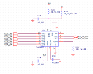
请在下面找到代码和原理图。 对于通道0、我能够读取数字数据。 但是、当我将模拟通道更改为通道1时、我无法读取通道1数据。 即使对通道1进行了通道配置、我也会获得相同的通道0数据。
连接了 Sch
通道0配置代码:
a)头文件
/* system_status 寄存器*/
#define system_status_address 0x00
#define SYSTEM_STATUS_DEFAULT 0x80
/* SEQ_STATUS 字段*/
#define SEQ_STATUS_MASK 0x40
#define SEQ_STATUS_STOPPED 默认为0x00 //
#define SEQ_STATUS_Running 0x40
/* I2C_SPEED 字段*/
#define I2C_SPEED_MASK 0x20
#define I2C_SPEED_NORMAL 默认为0x00 //
#define I2C_SPEED_HIGH 0x20
/* OSR_DONE 字段*/
#define OSR_DONE_MASK 0x08
#define OSR_DONE 等待 默认为0x00 //
#define OSR_DONE_COMPLETE 0x08
/* CRC_ERR_FUSE 字段*/
#define CRC_ERR_FUSE_MASK 0x04
#define CRC_ERR_FUSE_OK 默认为0x00 //
#define CRC_ERR_FUSE_ERROR 0x04
/* CRC_ERR_IN 字段*/
#define CRC_ERR_IN_MASK 0x02
#define CRC_ERR_IN_OK 默认为0x00 //
#define CRC_ERR_IN_ERROR 0x02
/* BOR 字段*/
#define BOR_MASK 0x01
#define BOR_OK 0x00
#define BOR_ERROR 0x01 //默认值
/*寄存器0x01 (General_CFG)定义
*|---------------------------------------------------------------- |
*| 位7 | 位6 | 位5 | 位4 | 位3 | 位2 | 位1 | 位0 |
*|---------------------------------------------------------------- |
*| RESERV[3:0] | CNVST | CH_RST | CAL | RST |
*|---------------------------------------------------------------- |
*
/* General_CFG 寄存器*/
#define General_CFG_ADDRESS 0x01
#define General_CFG_DEFAULT 0x00
/* CNVST 字段*/
#define CNVST_MASK 0x08
#define CNVST_NORMAL SCL_LEADDETLED_ 默认为0x00 //
#define CNVST_START_NO_LEVN 0x08
/* CH_RST 字段*/
#define CH_RST_MASK 0x04
#define CH_RST_NORMAL 默认为0x00 //
#define CH_RST_FORCE_AIN 0x04
/* CAL (校准)字段*/
#define CAL_MASK 0x02
#define CAL_COMPLETE 默认为0x00 //
#define CAL_START 0x02
/* RST 字段*/
#define RST_MASK 0x01
#define RST_COMPLETE 默认为0x00 //
#define RST_START 0x01
/*寄存器0x02 (DATA_CFG)定义
*|---------------------------------------------------------------- |
*| 位7 | 位6 | 位5 | 位4 | 位3 | 位2 | 位1 | 位0 |
*|---------------------------------------------------------------- |
*| fix_PAT | 保留 | append_status[1:0] | 保留[3:0] |
*|---------------------------------------------------------------- |
*
/* DATA_CFG 寄存器*/
#define DATA_CFG_ADDRESS 0x02
#define DATA_CFG_DEFAULT 0x00
/* FIX_PAT 字段*/
#define FIX_PAT_MASK 0x80
#define FIX_PAT_NORMAL 默认为0x00 //
#define FIX_PAT_ENABLE 0x80
/* append_status 字段*/
#define append_status_mask 0x30
#define append_status_disable 默认为0x00 //
#define append_status_ID 0x10
#define append_status_only 0x20
/*寄存器0x03 (OSR_CFG)定义
*|---------------------------------------------------------------- |
*| 位7 | 位6 | 位5 | 位4 | 位3 | 位2 | 位1 | 位0 |
*|---------------------------------------------------------------- |
*| RESERV[4:0] | OSR[2:0] |
*|---------------------------------------------------------------- |
*
/* OSR_CFG 寄存器*/
#define OSR_CFG_ADDRESS 0x03
#define OSR_CFG_DEFAULT 0x00
/* OSR 字段*/
#define OSR_MASK 0x07
#define OSR_1 默认为0x00 //
#define OSR_2 0x01
#define OSR_4 0x02
#define OSR_8 0x03
#define OSR_16 0x04
#define OSR_32 0x05
#define OSR_64 0x06
#define OSR_128 0x07
/*寄存器0x04 (OPMODE_CFG)定义
*|---------------------------------------------------------------- |
*| 位7 | 位6 | 位5 | 位4 | 位3 | 位2 | 位1 | 位0 |
*|---------------------------------------------------------------- |
*| 保留[2:0] | OSC_SEL | CLK_DIV[3:0] |
*|---------------------------------------------------------------- |
*
/* OPMODE_CFG 寄存器*/
#define OPMODE_CFG_ADDRESS 0x04
#define OPMODE_CFG_DEFAULT 0x00
/* OSC_SEL 字段*/
#define OSC_SEL_MASK 0x10
#define OSC_SEL_HIGH_SPEED 默认为0x00 //
#define OSC_SEL_LOW_POWER 0x10
/*寄存器0x05 (PIN_CFG)定义
*|---------------------------------------------------------------- |
*| 位7 | 位6 | 位5 | 位4 | 位3 | 位2 | 位1 | 位0 |
*|---------------------------------------------------------------- |
*| PIN_CFG[7:0] |
*|---------------------------------------------------------------- |
*
/* PIN_CFG 寄存器*/
#define PIN_CFG_ADDRESS 0x05
#define PIN_CFG_DEFAULT 0x00
/* PIN_CFG 域*/
#define PIN_CFG_MASK 0xFF
#define PIN_CFG_AIN0 0x01
#define PIN_CFG_AIN1 0x02
#define PIN_CFG_AIN2 0x04
#define PIN_CFG_AIN3 0x08
#define PIN_CFG_AIN4 0x10
#define PIN_CFG_AIN5 0x20
#define PIN_CFG_AIN6 0x40
#define PIN_CFG_AIN7 0x80
/*寄存器0x07 (GPIO_CFG)定义
*|---------------------------------------------------------------- |
*| 位7 | 位6 | 位5 | 位4 | 位3 | 位2 | 位1 | 位0 |
*|---------------------------------------------------------------- |
*| GPIO_CFG[7:0] |
*|---------------------------------------------------------------- |
*
/* GPIO_CFG 寄存器*/
#define GPIO_CFG_ADDRESS 0x07
#define GPIO_CFG_DEFAULT 0x00
/* GPIO_CFG 字段*/
#define GPIO_CFG_MASK 0xFF
#define GPIO_CFG_GPO0 0x01
#define GPIO_CFG_GPO1 0x02
#define GPIO_CFG_GPO2 0x04
#define GPIO_CFG_GPO3 0x08
#define GPIO_CFG_GPO4 0x10
#define GPIO_CFG_GPO5 0x20
#define GPIO_CFG_GPO6 0x40
#define GPIO_CFG_GPO7 0x80
/*寄存器0x09 (GPO_DRIVE_CFG)定义
*|---------------------------------------------------------------- |
*| 位7 | 位6 | 位5 | 位4 | 位3 | 位2 | 位1 | 位0 |
*|---------------------------------------------------------------- |
*| GPO_DRIVE_CFG[7:0] |
*|---------------------------------------------------------------- |
*
/* GPO_DRIVE_CFG 寄存器*/
#define GPO_DRIVE_CFG_ADDRESS 0x09
#define GPO_DRIVE_CFG_DEFAULT 0x00
/* GPO_DRIVE_CFG 字段*/
#define GPO_DRIVE_CFG_MASK 0xFF
#define GPO_DRIVE_CFG_GPO0 0x01
#define GPO_DRIVE_CFG_GPO1 0x02
#define GPO_DRIVE_CFG_GPO2 0x04
#define GPO_DRIVE_CFG_GPO3 0x08
#define GPO_DRIVE_CFG_GPO4 0x10
#define GPO_DRIVE_CFG_GPO5 0x20
#define GPO_DRIVE_CFG_GPO6 0x40
#define GPO_DRIVE_CFG_GPO7 0x80
/*寄存器0x0B (GPO_VALUE)定义
*|---------------------------------------------------------------- |
*| 位7 | 位6 | 位5 | 位4 | 位3 | 位2 | 位1 | 位0 |
*|---------------------------------------------------------------- |
*| GPO_Value[7:0] |
*|---------------------------------------------------------------- |
*
/* GPO_VALUE 寄存器*/
#define GPO_value_address 0x0B
#define GPO_value_default 0x00
/* GPO_VALUE 域*/
#define GPO_value_mask 0xFF
#define GPO_Value_GPO0_HIGH 0x01
#define GPO_value_GPO1_HIGH 0x02
#define GPO_Value_GPO2_HIGH 0x04
#define GPO_Value_GPO3_HIGH 0x08
#define GPO_Value_GPO4_HIGH 0x10
#define GPO_Value_GPO5_HIGH 0x20
#define GPO_Value_GPO6_HIGH 0x40
#define GPO_Value_GPO7_HIGH 0x80
/*寄存器0x0D (GPI_VALUE)定义
*|---------------------------------------------------------------- |
*| 位7 | 位6 | 位5 | 位4 | 位3 | 位2 | 位1 | 位0 |
*|---------------------------------------------------------------- |
*| GPI_Value[7:0] |
*|---------------------------------------------------------------- |
*
/* GPI_VALUE 寄存器*/
#define GPI_value_address 0x0D
#define GPI_value_default 0x00
/* GPI_VALUE 域*/
#define GPI_value_mask 0xFF
#define GPI_Value_GPI0_HIGH 0x01
#define GPI_value_GPI1_HIGH 0x02
#define GPI_Value_GPI2_HIGH 0x04
#define GPI_value_GPI3_HIGH 0x08
#define GPI_value_GPI4_HIGH 0x10
#define GPI_value_GPI5_HIGH 0x20
#define GPI_value_GPI6_HIGH 0x40
#define GPI_value_GPI7_HIGH 0x80
/*寄存器0x10 (SEQUEST_CFG)定义
*|---------------------------------------------------------------- |
*| 位7 | 位6 | 位5 | 位4 | 位3 | 位2 | 位1 | 位0 |
*|---------------------------------------------------------------- |
*| RESERV[2:0] | SEQ_START | RESERV[1:0] | SEQ_MODE[1:0] |
*|---------------------------------------------------------------- |
*
/* SEQUEST_CFG 寄存器*/
#define SEQUENSE_CFG_ADDRESS 0x10
#define SEQUENSE_CFG_DEFAULT 0x00
/* SEQ_START 字段*/
#define SEQ_START_MASK 0x10
#define SEQ_START_END 默认为0x00 //
#define SEQ_START_ASSEND 0x10
/* SEQ_MODE 字段*/
#define SEQ_MODE_MASK 0x03
#define SEQ_MODE_MANUAL 默认为0x00 //
#define SEQ_MODE_AUTO 0x01
/*寄存器0x11 (MANUAL_CH_SEL)定义
*|---------------------------------------------------------------- |
*| 位7 | 位6 | 位5 | 位4 | 位3 | 位2 | 位1 | 位0 |
*|---------------------------------------------------------------- |
*| 保留[3:0] | MANUAL_Chid[3:0] |
*|---------------------------------------------------------------- |
*
/* MANUAL_CH_SEL 寄存器*/
#define MANUAL_CH_SEL_ADDRESS 0x11
#define MANUAL_CH_SEL_DEFAULT 0x00
/* manual_chid 字段*/
#define MANUAL_Chid_MASK 0x0F
#define MANUAL_Chid_AIN0 默认为0x00 //
#define MANUAL_Chid_AIN1 0x01
#define MANUAL_Chid_AIN2 0x02
#define MANUAL_Chid_AIN3 0x03
#define MANUAL_Chid_AIN4 0x04
#define MANUAL_Chid_AIN5 0x05
#define MANUAL_Chid_AIN6 0x06
#define MANUAL_Chid_AIN7 0x07
/*寄存器0x12 (AUTO_SEQ_CH_SEL)定义
*|---------------------------------------------------------------- |
*| 位7 | 位6 | 位5 | 位4 | 位3 | 位2 | 位1 | 位0 |
*|---------------------------------------------------------------- |
*| AUTO_SEQ_CH_SEL[7:0] |
*|---------------------------------------------------------------- |
*
/* AUTO_SEQ_CH_SEL 寄存器*/
#define AUTO_SEQ_CH_SEL_ADDRESS 0x12
#define AUTO_SEQ_CH_SEL_DEFAULT 0x00
/* AUTO_SEQ_CH_SEL 字段*/
#define AUTO_SEQ_CH_SEL_MASK 0xFF
#define AUTO_SEQ_CH_SEL_AIN0 0x01
#define AUTO_SEQ_CH_SEL_AIN1 0x02
#define AUTO_SEQ_CH_SEL_AIN2 0x04
#define AUTO_SEQ_CH_SEL_AIN3 0x08
#define AUTO_SEQ_CH_SEL_AIN4 0x10
#define AUTO_SEQ_CH_SEL_AIN5 0x20
#define AUTO_SEQ_CH_SEL_AIN6 0x40
#define AUTO_SEQ_CH_SEL_AIN7 0x80
#define SLAVE_ADDRESS_TLA (0x13 <<1)
void adc_tla2528_test (void);
#endif /* TLA2528_H_*
b) c 源文件
#include "adc_tla2528.h"
#include "string.h"
#include "USART.h"
#include "i2c.h"
uint8_t rx_buf[100];
void adc_tla2528_test (void)
{
unsigned buffchar 1[2];
buff1[0]= system_status_address;
buff1[1]= system_status_default;
unsigned buffchar 2[2];
buff2[0]= General_CFG_ADDRESS;
buff2[1]= General_CFG_DEFAULT;
unsigned buffchar 3[2];
buff3[0]= DATA_CFG_ADDRESS;
buff3[1]= DATA_CFG_DEFAULT;
unsigned buffchar 4[2];
buff4[0]= OSR_CFG_ADDRESS;
buff4[1]= OSR_CFG_DEFAULT;
unsigned buffchar 5[2];
buff5[0]= OPMODE_CFG_ADDRESS;
buff5[1]= OPMODE_CFG_DEFAULT;
unsigned buffchar 6[2];
buff6[0]= PIN_CFG_ADDRESS;
buff6[1]= PIN_CFG_DEFAULT;
unsigned buffchar 7[2];
buff7[0]= GPIO_CFG_ADDRESS;
buff7[1]= GPIO_CFG_DEFAULT;
unsigned buffchar 8[2];
buff8[0]= GPO_DRIVE_CFG_ADDRESS;
buff8[1]= GPO_DRIVE_CFG_DEFAULT;
unsigned buffchar 9[2];
buff9[0]= GPO_value_address;
buff9[1]= GPO_value_default;
unsigned buffchar 10[2];
buff10[0]= GPI_value_address;
buff10[1]= GPO_value_default;
unsigned buffchar 11[2];
buff11[0]= SEQUEST_CFG_ADDRESS;
buff11[1]= seque_CFG_DEFAULT;
unsigned buffchar 12[2];
buff12[0]= MANUAL_CH_SEL_ADDRESS;
buff12[1]= MANUAL_CH_SEL_DEFAULT;
unsigned buffchar 13[2];
buff13[0]= AUTO_SEQ_CH_SEL_ADDRESS;
buff13[1]= AUTO_SEQ_CH_SEL_DEFAULT;
HAL_I2C_Master_transmit (&hi2c1、slave_address_TLA、(uint8_t *) buff1、2、100);
HAL_DELAY (1);
HAL_I2C_Master_transmit (&hi2c1、slave_address_TLA、(uint8_t *) buff2、2、100);
HAL_DELAY (1);
HAL_I2C_Master_transmit (&hi2c1、slave_address_TLA、(uint8_t *) buff3、2、100);
HAL_DELAY (1);
HAL_I2C_Master_transmit (&hi2c1、slave_address_TLA、(uint8_t *) buff4、2、100);
HAL_DELAY (1);
HAL_I2C_Master_transmit (&hi2c1、slave_address_TLA、(uint8_t *) buff5、2、100);
HAL_DELAY (1);
HAL_I2C_Master_transmit (&hi2c1、slave_address_TLA、(uint8_t *) buff6、2、100);
HAL_DELAY (1);
HAL_I2C_Master_transmit (&hi2c1、slave_address_TLA、(uint8_t *) buff7、2、100);
HAL_DELAY (1);
HAL_I2C_Master_transmit (&hi2c1、slave_address_TLA、(uint8_t *) buff8、2、100);
HAL_DELAY (1);
HAL_I2C_Master_transmit (&hi2c1、slave_address_TLA、(uint8_t *) buff9、2、100);
HAL_DELAY (1);
HAL_I2C_Master_transmit (&hi2c1、slave_address_TLA、(uint8_t *) buff10、2、100);
HAL_DELAY (1);
HAL_I2C_Master_transmit (&hi2c1、slave_address_TLA、(uint8_t *) buff11、2、100);
HAL_DELAY (1);
HAL_I2C_Master_transmit (&hi2c1、slave_address_TLA、(uint8_t *) buff12、2、100);
HAL_DELAY (1);
HAL_I2C_Master_transmit (&hi2c1、slave_address_TLA、(uint8_t *) buff13、2、100);
HAL_DELAY (1);
HAL_I2C_Master_Receive (&hi2c1、slave_address_TLA、(uint8_t *) rx_Buf、3、100);
}
2.通道1配置的代码
#define system_status_address 0x00
#define SYSTEM_STATUS_DEFAULT 0x80
/* SEQ_STATUS 字段*/
#define SEQ_STATUS_MASK 0x40
#define SEQ_STATUS_STOPPED 默认为0x00 //
#define SEQ_STATUS_Running 0x40
/* I2C_SPEED 字段*/
#define I2C_SPEED_MASK 0x20
#define I2C_SPEED_NORMAL 默认为0x00 //
#define I2C_SPEED_HIGH 0x20
/* OSR_DONE 字段*/
#define OSR_DONE_MASK 0x08
#define OSR_DONE 等待 默认为0x00 //
#define OSR_DONE_COMPLETE 0x08
/* CRC_ERR_FUSE 字段*/
#define CRC_ERR_FUSE_MASK 0x04
#define CRC_ERR_FUSE_OK 默认为0x00 //
#define CRC_ERR_FUSE_ERROR 0x04
/* CRC_ERR_IN 字段*/
#define CRC_ERR_IN_MASK 0x02
#define CRC_ERR_IN_OK 默认为0x00 //
#define CRC_ERR_IN_ERROR 0x02
/* BOR 字段*/
#define BOR_MASK 0x01
#define BOR_OK 0x00
#define BOR_ERROR 0x01 //默认值
/*寄存器0x01 (General_CFG)定义
*|---------------------------------------------------------------- |
*| 位7 | 位6 | 位5 | 位4 | 位3 | 位2 | 位1 | 位0 |
*|---------------------------------------------------------------- |
*| RESERV[3:0] | CNVST | CH_RST | CAL | RST |
*|---------------------------------------------------------------- |
*
/* General_CFG 寄存器*/
#define General_CFG_ADDRESS 0x01
#define General_CFG_DEFAULT 0x00
/* CNVST 字段*/
#define CNVST_MASK 0x08
#define CNVST_NORMAL SCL_LEADDETLED_ 默认为0x00 //
#define CNVST_START_NO_LEVN 0x08
/* CH_RST 字段*/
#define CH_RST_MASK 0x04
#define CH_RST_NORMAL 默认为0x00 //
#define CH_RST_FORCE_AIN 0x04
/* CAL (校准)字段*/
#define CAL_MASK 0x02
#define CAL_COMPLETE 默认为0x00 //
#define CAL_START 0x02
/* RST 字段*/
#define RST_MASK 0x01
#define RST_COMPLETE 默认为0x00 //
#define RST_START 0x01
/*寄存器0x02 (DATA_CFG)定义
*|---------------------------------------------------------------- |
*| 位7 | 位6 | 位5 | 位4 | 位3 | 位2 | 位1 | 位0 |
*|---------------------------------------------------------------- |
*| fix_PAT | 保留 | append_status[1:0] | 保留[3:0] |
*|---------------------------------------------------------------- |
*
/* DATA_CFG 寄存器*/
#define DATA_CFG_ADDRESS 0x02
#define DATA_CFG_DEFAULT 0x00
/* FIX_PAT 字段*/
#define FIX_PAT_MASK 0x80
#define FIX_PAT_NORMAL 默认为0x00 //
#define FIX_PAT_ENABLE 0x80
/* append_status 字段*/
#define append_status_mask 0x30
#define append_status_disable 默认为0x00 //
#define append_status_ID 0x10
#define append_status_only 0x20
/*寄存器0x03 (OSR_CFG)定义
*|---------------------------------------------------------------- |
*| 位7 | 位6 | 位5 | 位4 | 位3 | 位2 | 位1 | 位0 |
*|---------------------------------------------------------------- |
*| RESERV[4:0] | OSR[2:0] |
*|---------------------------------------------------------------- |
*
/* OSR_CFG 寄存器*/
#define OSR_CFG_ADDRESS 0x03
#define OSR_CFG_DEFAULT 0x00
/* OSR 字段*/
#define OSR_MASK 0x07
#define OSR_1 默认为0x00 //
#define OSR_2 0x01
#define OSR_4 0x02
#define OSR_8 0x03
#define OSR_16 0x04
#define OSR_32 0x05
#define OSR_64 0x06
#define OSR_128 0x07
/*寄存器0x04 (OPMODE_CFG)定义
*|---------------------------------------------------------------- |
*| 位7 | 位6 | 位5 | 位4 | 位3 | 位2 | 位1 | 位0 |
*|---------------------------------------------------------------- |
*| 保留[2:0] | OSC_SEL | CLK_DIV[3:0] |
*|---------------------------------------------------------------- |
*
/* OPMODE_CFG 寄存器*/
#define OPMODE_CFG_ADDRESS 0x04
#define OPMODE_CFG_DEFAULT 0x00
/* OSC_SEL 字段*/
#define OSC_SEL_MASK 0x10
#define OSC_SEL_HIGH_SPEED 默认为0x00 //
#define OSC_SEL_LOW_POWER 0x10
/*寄存器0x05 (PIN_CFG)定义
*|---------------------------------------------------------------- |
*| 位7 | 位6 | 位5 | 位4 | 位3 | 位2 | 位1 | 位0 |
*|---------------------------------------------------------------- |
*| PIN_CFG[7:0] |
*|---------------------------------------------------------------- |
*
/* PIN_CFG 寄存器*/
#define PIN_CFG_ADDRESS 0x05
#define PIN_CFG_DEFAULT 0x00
/* PIN_CFG 域*/
#define PIN_CFG_MASK 0xFF
#define PIN_CFG_AIN0 0x01
#define PIN_CFG_AIN1 0x02
#define PIN_CFG_AIN2 0x04
#define PIN_CFG_AIN3 0x08
#define PIN_CFG_AIN4 0x10
#define PIN_CFG_AIN5 0x20
#define PIN_CFG_AIN6 0x40
#define PIN_CFG_AIN7 0x80
/*寄存器0x07 (GPIO_CFG)定义
*|---------------------------------------------------------------- |
*| 位7 | 位6 | 位5 | 位4 | 位3 | 位2 | 位1 | 位0 |
*|---------------------------------------------------------------- |
*| GPIO_CFG[7:0] |
*|---------------------------------------------------------------- |
*
/* GPIO_CFG 寄存器*/
#define GPIO_CFG_ADDRESS 0x07
#define GPIO_CFG_DEFAULT 0x00
/* GPIO_CFG 字段*/
#define GPIO_CFG_MASK 0xFF
#define GPIO_CFG_GPO0 0x01
#define GPIO_CFG_GPO1 0x02
#define GPIO_CFG_GPO2 0x04
#define GPIO_CFG_GPO3 0x08
#define GPIO_CFG_GPO4 0x10
#define GPIO_CFG_GPO5 0x20
#define GPIO_CFG_GPO6 0x40
#define GPIO_CFG_GPO7 0x80
/*寄存器0x09 (GPO_DRIVE_CFG)定义
*|---------------------------------------------------------------- |
*| 位7 | 位6 | 位5 | 位4 | 位3 | 位2 | 位1 | 位0 |
*|---------------------------------------------------------------- |
*| GPO_DRIVE_CFG[7:0] |
*|---------------------------------------------------------------- |
*
/* GPO_DRIVE_CFG 寄存器*/
#define GPO_DRIVE_CFG_ADDRESS 0x09
#define GPO_DRIVE_CFG_DEFAULT 0x00
/* GPO_DRIVE_CFG 字段*/
#define GPO_DRIVE_CFG_MASK 0xFF
#define GPO_DRIVE_CFG_GPO0 0x01
#define GPO_DRIVE_CFG_GPO1 0x02
#define GPO_DRIVE_CFG_GPO2 0x04
#define GPO_DRIVE_CFG_GPO3 0x08
#define GPO_DRIVE_CFG_GPO4 0x10
#define GPO_DRIVE_CFG_GPO5 0x20
#define GPO_DRIVE_CFG_GPO6 0x40
#define GPO_DRIVE_CFG_GPO7 0x80
/*寄存器0x0B (GPO_VALUE)定义
*|---------------------------------------------------------------- |
*| 位7 | 位6 | 位5 | 位4 | 位3 | 位2 | 位1 | 位0 |
*|---------------------------------------------------------------- |
*| GPO_Value[7:0] |
*|---------------------------------------------------------------- |
*
/* GPO_VALUE 寄存器*/
#define GPO_value_address 0x0B
#define GPO_value_default 0x00
/* GPO_VALUE 域*/
#define GPO_value_mask 0xFF
#define GPO_Value_GPO0_HIGH 0x01
#define GPO_value_GPO1_HIGH 0x02
#define GPO_Value_GPO2_HIGH 0x04
#define GPO_Value_GPO3_HIGH 0x08
#define GPO_Value_GPO4_HIGH 0x10
#define GPO_Value_GPO5_HIGH 0x20
#define GPO_Value_GPO6_HIGH 0x40
#define GPO_Value_GPO7_HIGH 0x80
/*寄存器0x0D (GPI_VALUE)定义
*|---------------------------------------------------------------- |
*| 位7 | 位6 | 位5 | 位4 | 位3 | 位2 | 位1 | 位0 |
*|---------------------------------------------------------------- |
*| GPI_Value[7:0] |
*|---------------------------------------------------------------- |
*
/* GPI_VALUE 寄存器*/
#define GPI_value_address 0x0D
#define GPI_value_default 0x00
/* GPI_VALUE 域*/
#define GPI_value_mask 0xFF
#define GPI_Value_GPI0_HIGH 0x01
#define GPI_value_GPI1_HIGH 0x02
#define GPI_Value_GPI2_HIGH 0x04
#define GPI_value_GPI3_HIGH 0x08
#define GPI_value_GPI4_HIGH 0x10
#define GPI_value_GPI5_HIGH 0x20
#define GPI_value_GPI6_HIGH 0x40
#define GPI_value_GPI7_HIGH 0x80
/*寄存器0x10 (SEQUEST_CFG)定义
*|---------------------------------------------------------------- |
*| 位7 | 位6 | 位5 | 位4 | 位3 | 位2 | 位1 | 位0 |
*|---------------------------------------------------------------- |
*| RESERV[2:0] | SEQ_START | RESERV[1:0] | SEQ_MODE[1:0] |
*|---------------------------------------------------------------- |
*
/* SEQUEST_CFG 寄存器*/
#define SEQUENSE_CFG_ADDRESS 0x10
#define SEQUENSE_CFG_DEFAULT 0x00
/* SEQ_START 字段*/
#define SEQ_START_MASK 0x10
#define SEQ_START_END 默认为0x00 //
#define SEQ_START_ASSEND 0x10
/* SEQ_MODE 字段*/
#define SEQ_MODE_MASK 0x03
#define SEQ_MODE_MANUAL 默认为0x00 //
#define SEQ_MODE_AUTO 0x01
/*寄存器0x11 (MANUAL_CH_SEL)定义
*|---------------------------------------------------------------- |
*| 位7 | 位6 | 位5 | 位4 | 位3 | 位2 | 位1 | 位0 |
*|---------------------------------------------------------------- |
*| 保留[3:0] | MANUAL_Chid[3:0] |
*|---------------------------------------------------------------- |
*
/* MANUAL_CH_SEL 寄存器*/
#define MANUAL_CH_SEL_ADDRESS 0x11
#define MANUAL_CH_SEL_DEFAULT 0x01 //通道1已配置
/* manual_chid 字段*/
#define MANUAL_Chid_MASK 0x0F
#define MANUAL_Chid_AIN0 默认为0x00 //
#define MANUAL_Chid_AIN1 0x01
#define MANUAL_Chid_AIN2 0x02
#define MANUAL_Chid_AIN3 0x03
#define MANUAL_Chid_AIN4 0x04
#define MANUAL_Chid_AIN5 0x05
#define MANUAL_Chid_AIN6 0x06
#define MANUAL_Chid_AIN7 0x07
/*寄存器0x12 (AUTO_SEQ_CH_SEL)定义
*|---------------------------------------------------------------- |
*| 位7 | 位6 | 位5 | 位4 | 位3 | 位2 | 位1 | 位0 |
*|---------------------------------------------------------------- |
*| AUTO_SEQ_CH_SEL[7:0] |
*|---------------------------------------------------------------- |
*
/* AUTO_SEQ_CH_SEL 寄存器*/
#define AUTO_SEQ_CH_SEL_ADDRESS 0x12
#define AUTO_SEQ_CH_SEL_DEFAULT 0x00
/* AUTO_SEQ_CH_SEL 字段*/
#define AUTO_SEQ_CH_SEL_MASK 0xFF
#define AUTO_SEQ_CH_SEL_AIN0 0x01
#define AUTO_SEQ_CH_SEL_AIN1 0x02
#define AUTO_SEQ_CH_SEL_AIN2 0x04
#define AUTO_SEQ_CH_SEL_AIN3 0x08
#define AUTO_SEQ_CH_SEL_AIN4 0x10
#define AUTO_SEQ_CH_SEL_AIN5 0x20
#define AUTO_SEQ_CH_SEL_AIN6 0x40
#define AUTO_SEQ_CH_SEL_AIN7 0x80
#define SLAVE_ADDRESS_TLA (0x13 <<1)
void adc_tla2528_test (void);
#endif /* TLA2528_H_*
b) C 源代码文件保持不变
请建议
--
Phrutvi
Bharat Electronics Limited
班加罗尔