


请注意,本文内容源自机器翻译,可能存在语法或其它翻译错误,仅供参考。如需获取准确内容,请参阅链接中的英语原文或自行翻译。
器件型号:ADS8691 您好!
我对您的 ADC 有一些问题:ADS8691IPW。
主要问题是缺乏可靠的工作。
它通过跳线连接到 STM32F411E-DISCOS 开发板。
ADC 本身焊接在执行板上以用于调试。
它主要内置于具有四个菊花链单元的定制 PCB 中、但问题是类似的。 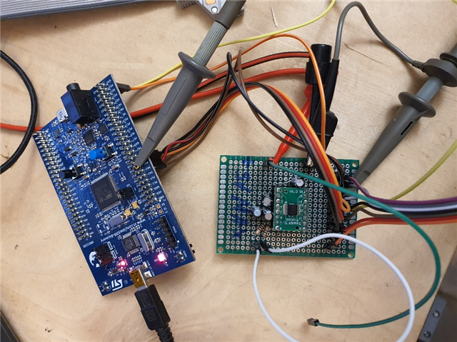
STM 由 USB 供电、ADC 模拟端和数字端通过 Keithley SMU 提供5V 电压。
使用1uF 电解电容器进行去耦。
我已经通过具有类似效果的多个 ADC 进行了迭代。
问题是它仅在连接示波器时起作用。
但在重新设置 STM 或将接地端连接到逻辑分析仪或将数字引脚连接到逻辑分析仪后、或一段时间后、它会停止工作。
我可以通过以下方式使其正常工作:
为 ADC 重置跳线、
断开跳线与逻辑分析仪的连接、
断开逻辑分析仪的接地、
重新连接到逻辑分析仪、
和许多其他组合。 
定制 PCB ADC 原理图: 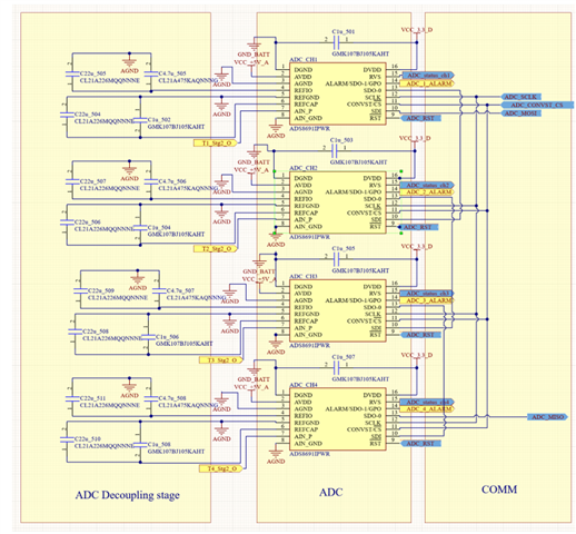
在定制 PCB 上、由于寄生引起的过冲和下冲显著降低。
绕过是根据指南进行的。
请注意、还有一个接地引线电感、它看起来会更糟。
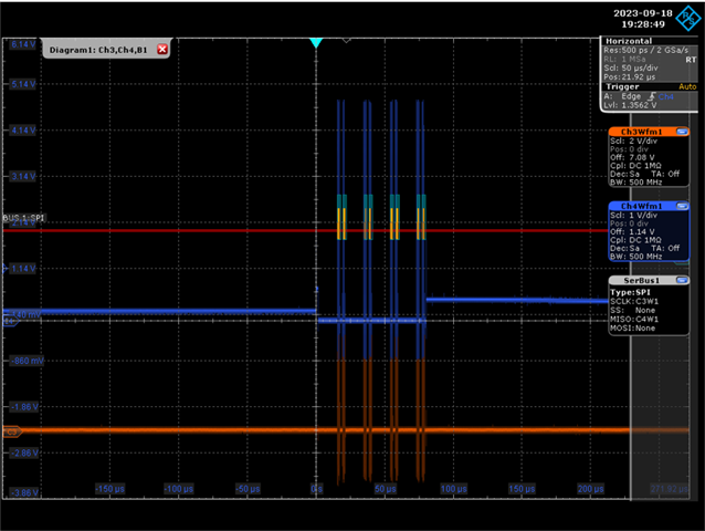
(在所有屏幕中、示波器在 SPI 总线上触发)
当它工作时、数据会清晰地显示 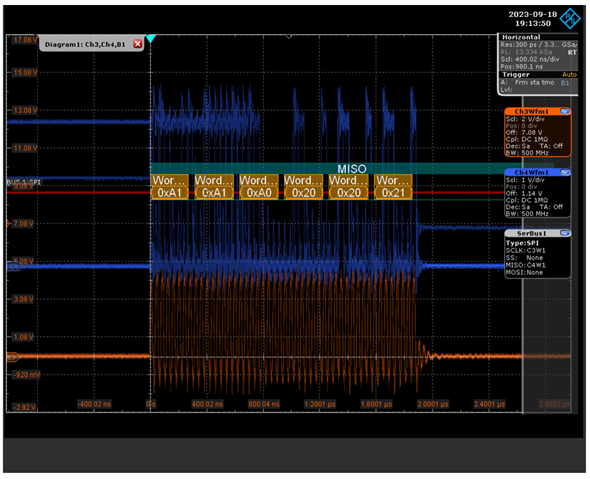
有时在重置后、看起来是这样的: 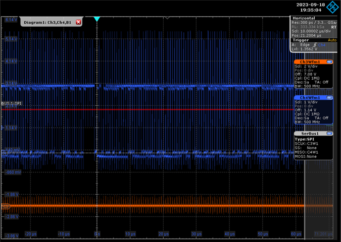
或者根本无法正常工作。
我还在 MCU 以及靠近 ADC 的硬件中尝试了上拉和下拉电阻。
此外、还测试了不同的 CLK 速度。
代码:
来自 main 的零件:
void HAL_GPIO_EXTI_Callback(uint16_t GPIO_Pin)
{
	if(GPIO_Pin == ADC_ALARM_Pin)
	{
	   //This block will be triggered after pin activated.
		if(BUTTON_Pin == 1)
		{
			for(int i = 0; i < 4; i++)
			{
			read_hword_data();
	    	char *msg = "ADC Alarm working\r\n";
	        HAL_UART_Transmit(&huart2, msg, sizeof(msg), 100);
			}
		}
	}
}

void HAL_SPI_RxCpltCallback(SPI_HandleTypeDef * hspi)
{
    HAL_SPI_Receive_DMA(&hspi1, RX_Buffer, sizeof(RX_Buffer));
    if(sample < 50000)
    {
    	read_adc_data(&adc_handle, RX_Buffer, sample);
    	sample++;
    }
    else if(sample == 50000)
    {
    	char *msg = "50 000 samples gathered\r\n";
        HAL_UART_Transmit(&huart2, msg, sizeof(msg), 100);
    }

}
自定义库:
struct adc_state adc_init() {
	struct adc_state state;
/*
	for(uint16_t i=0; i<12500; i++) state.data0[i] = '\0';
	for(uint16_t i=0; i<12500; i++) state.data1[i] = '\0';
	for(uint16_t i=0; i<12500; i++) state.data2[i] = '\0';
	for(uint16_t i=0; i<12500; i++) state.data3[i] = '\0';
*/
	return state;
}

/*
 * 11000_xx_<9-bit address>_ <16-bit data>
 * Command used to clear any (or a group of) bits of a register.
 * Any bit marked 1 in the data field results in that particular bit of the specified register being reset to 0, leaving the other bits unchanged.
 * Half-word command (that is, the command functions on 16 bits at a time).
 * LSB of the 9-bit address is always ignored and considered as 0b.(2)
 */
void clear_hword(char *reg)
{
	char command[16];
	sprintf(command, "11000000%s", reg);
	HAL_SPI_Transmit(&hspi1, command, sizeof(command), 0);
}

/*
 * 11001_xx_<9-bit address>_ 00000000_00000000
 * Command used to perform a 16-bit read operation.
 * Half-word command (that is, the device outputs 16 bits of register data at a time).
 * LSB of the 9-bit address is always ignored and considered as 0b.
 * Upon receiving this command, the device sends out 16 bits of the register in the next frame.
 */
void read_hword(char *reg)
{
	char x[8] = "00000000";
	char command[16];
	sprintf(command, "11001000%s", reg);
	HAL_SPI_Transmit(&hspi1, command, sizeof(command), 0);
	HAL_SPI_Transmit(&hspi1, x, sizeof(x), 0);
}


void read_hword_data()
{
	if(HAL_GPIO_ReadPin(GPIOA, GPIO_PIN_3) == 1)
		{
			HAL_GPIO_WritePin(GPIOA, GPIO_PIN_4, GPIO_PIN_RESET);
			for(int i = 0; i < 4; i++)
			{
				read_hword(DATAOUT_CTL_REG);
			}
			HAL_GPIO_WritePin(GPIOA, GPIO_PIN_4, GPIO_PIN_SET);
		}
}

/*
 * 01001_xx_<9-bit address>_ 00000000_00000000
 * Same as the READ_HWORD except that only eight bits of the register (byte read) are returned in the next frame.
*/
void read_word(char *reg)
{
	char command[16];
	sprintf(command, "01001000%s", reg);
	HAL_SPI_Transmit(&hspi1, command, sizeof(command), 0);
}

/*
 * 11010_00_<9-bit address>_ <16-bit data>
 * Half-word write command (two bytes of input data are written into the specified address).
 * LSB of the 9-bit address is always ignored and considered as 0b.
 *
 * 11010_01_<9-bit address>_ <16-bit data>
 * Half-word write command.
 * LSB of the 9-bit address is always ignored and considered as 0b.
 * With this command, only the MS byte of the 16-bit data word is written at the specified register address. The LS byte is ignored.
 *
 * 11010_10_<9-bit address>_ <16-bit data>
 * Half-word write command.
 * LSB of the 9-bit address is always ignored and considered as 0b.
 * With this command, only the LS byte of the 16-bit data word is written at the specified register address. The MS byte is ignored.
 */
void write_word(char *reg)
{
	char command[16];
	sprintf(command, "11010000%s", reg);
	HAL_SPI_Transmit(&hspi1, command, sizeof(command), 0);
}

/*
 * 11011_xx_<9-bit address>_ <16-bit data>
 * Command used to set any (or a group of) bits of a register.
 * Any bit marked 1 in the data field results in that particular bit of the specified register being set to 1, leaving the other bits unchanged.
 * Half-word command (that is, the command functions on 16 bits at a time).
 * LSB of the 9-bit address is always ignored and considered as 0b.
 */
void set_hword(char *reg)
{
	char command[16];
	sprintf(command, "11011000%s", reg);
	HAL_SPI_Transmit(&hspi1, command, sizeof(command), 0);
}

/*
 * Configuration described in the documentation in chapter "7.6 Register Maps" (p.48)
 * www.ti.com/.../ads8691.pdf
 */
void id_config()
{
	if(HAL_GPIO_ReadPin(GPIOA, GPIO_PIN_3) == 1)
	{
		HAL_GPIO_WritePin(GPIOA, GPIO_PIN_4, GPIO_PIN_RESET);
		for(int i = 0; i < 4; i++)
		{
			write_word(DEVICE_ID_REG);
			char command[16];
			sprintf(command,"0000000000000000");
			HAL_SPI_Transmit(&hspi1, command, sizeof(command), 10);
		}
		HAL_GPIO_WritePin(GPIOA, GPIO_PIN_4, GPIO_PIN_SET);
	}
}

/*
 * Configuration described in the documentation in chapter "7.6 Register Maps" (p.48)
 * www.ti.com/.../ads8691.pdf
 */
void reset_config()
{
	if(HAL_GPIO_ReadPin(GPIOA, GPIO_PIN_3) == 1)
	{
		HAL_GPIO_WritePin(GPIOA, GPIO_PIN_4, GPIO_PIN_RESET);
		for(int i = 0; i < 4; i++)
		{
			write_word(RST_PWRCTL_REG);
			char command[16];
			sprintf(command,"0100010100100000");
			HAL_SPI_Transmit(&hspi1, command, sizeof(command), 10);
		}
		HAL_GPIO_WritePin(GPIOA, GPIO_PIN_4, GPIO_PIN_SET);
	}
}

/*
 * Configuration described in the documentation in chapter "7.6 Register Maps" (p.48)
 * www.ti.com/.../ads8691.pdf
 */
void sdi_config()
{
	if(HAL_GPIO_ReadPin(GPIOA, GPIO_PIN_3) == 1)
	{
		HAL_GPIO_WritePin(GPIOA, GPIO_PIN_4, GPIO_PIN_RESET);
		for(int i = 0; i < 4; i++)
		{
			write_word(SDI_CTL_REG);
			char command[16];
			sprintf(command,"0000000000000000");
			HAL_SPI_Transmit(&hspi1, command, sizeof(command), 10);
		}
		HAL_GPIO_WritePin(GPIOA, GPIO_PIN_4, GPIO_PIN_SET);
	}
}

/*
 * Configuration described in the documentation in chapter "7.6 Register Maps" (p.48)
 * www.ti.com/.../ads8691.pdf
 */
void sdo_config()
{
	if(HAL_GPIO_ReadPin(GPIOA, GPIO_PIN_3) == 1)
	{
		HAL_GPIO_WritePin(GPIOA, GPIO_PIN_4, GPIO_PIN_RESET);
		for(int i = 0; i < 4; i++)
		{
			write_word(SDO_CTL_REG);
			char command[16];
			sprintf(command,"0000000100000000");
			HAL_SPI_Transmit(&hspi1, command, sizeof(command), 10);
		}
		HAL_GPIO_WritePin(GPIOA, GPIO_PIN_4, GPIO_PIN_SET);
	}
}

/*
 * Configuration described in the documentation in chapter "7.6 Register Maps" (p.48)
 * www.ti.com/.../ads8691.pdf
 */
void data_config()
{
	if(HAL_GPIO_ReadPin(GPIOA, GPIO_PIN_3) == 1)
	{
		HAL_GPIO_WritePin(GPIOA, GPIO_PIN_4, GPIO_PIN_RESET);
		for(int i = 0; i < 4; i++)
		{
			write_word(DATAOUT_CTL_REG);
			char command[16];
			sprintf(command,"0100110000000000");
			HAL_SPI_Transmit(&hspi1, command, sizeof(command), 10);
		}
		HAL_GPIO_WritePin(GPIOA, GPIO_PIN_4, GPIO_PIN_SET);
	}
}

/*
 * Configuration described in the documentation in chapter "7.6 Register Maps" (p.48)
 * www.ti.com/.../ads8691.pdf
 */
void ref_vol_config()
{
	if(HAL_GPIO_ReadPin(GPIOA, GPIO_PIN_3) == 1)
	{
		HAL_GPIO_WritePin(GPIOA, GPIO_PIN_4, GPIO_PIN_RESET);
		for(int i = 0; i < 4; i++)
		{
			write_word(RANGE_SEL_REG);
			char command[16];
			sprintf(command,"0000000000000000");
			HAL_SPI_Transmit(&hspi1, command, sizeof(command), 10);
		}
		HAL_GPIO_WritePin(GPIOA, GPIO_PIN_4, GPIO_PIN_SET);
	}
}

/*
 * Configuration described in the documentation in chapter "7.6 Register Maps" (p.48)
 * www.ti.com/.../ads8691.pdf
 */
void alarms_config()
{
	if(HAL_GPIO_ReadPin(GPIOA, GPIO_PIN_3) == 1)
	{
		HAL_GPIO_WritePin(GPIOA, GPIO_PIN_4, GPIO_PIN_RESET);
		for(int i = 0; i < 4; i++)
		{
			write_word(ALARM_REG);
			char command[16];
			sprintf(command,"0000110000000000");
			HAL_SPI_Transmit(&hspi1, command, sizeof(command), 10);
		}
		HAL_GPIO_WritePin(GPIOA, GPIO_PIN_4, GPIO_PIN_SET);
	}
}

/*
 * Configuration described in the documentation in chapter "7.6 Register Maps" (p.48)
 * www.ti.com/.../ads8691.pdf
 */
void alarmh_config()
{
	if(HAL_GPIO_ReadPin(GPIOA, GPIO_PIN_3) == 1)
	{
		HAL_GPIO_WritePin(GPIOA, GPIO_PIN_4, GPIO_PIN_RESET);
		for(int i = 0; i < 4; i++)
		{
			write_word(ALARM_H_TH_REG);
			char command[16];
			sprintf(command,"0000000000000000");
			HAL_SPI_Transmit(&hspi1, command, sizeof(command), 10);
		}
		HAL_GPIO_WritePin(GPIOA, GPIO_PIN_4, GPIO_PIN_SET);
	}
}

/*
 * Configuration described in the documentation in chapter "7.6 Register Maps" (p.48)
 * www.ti.com/.../ads8691.pdf
 */
void alarml_config()
{
	if(HAL_GPIO_ReadPin(GPIOA, GPIO_PIN_3) == 1)
	{
		HAL_GPIO_WritePin(GPIOA, GPIO_PIN_4, GPIO_PIN_RESET);
		for(int i = 0; i < 4; i++)
		{
			write_word(ALARM_L_TH_REG);
			char command[16];
			sprintf(command,"0000000000000000");
			HAL_SPI_Transmit(&hspi1, command, sizeof(command), 10);		}
		HAL_GPIO_WritePin(GPIOA, GPIO_PIN_4, GPIO_PIN_SET);
	}
}

// Initialization of all ADC's registers
void adc_config()
{
	id_config();
	reset_config();
	sdi_config();
	sdo_config();
	data_config();
	ref_vol_config();
	alarms_config();
	alarmh_config();
	alarml_config();

}

//
void read_adc_data(struct adc_state *state, uint8_t *val, uint16_t x)
{
	x = x/4;
	receiver_check(state, val, x);
	read_hword_data();

}

//
void receiver_check(struct adc_state *state, uint8_t *val, uint16_t x)
{
	int16_t data;
	data = (val[3] << 8) | val[2];
