请注意,本文内容源自机器翻译,可能存在语法或其它翻译错误,仅供参考。如需获取准确内容,请参阅链接中的英语原文或自行翻译。
器件型号:ADC12DJ5200RFEVM 主题中讨论的其他器件:ADC12DJ5200RF、 TI-JESD204-IP
您好!
现在、数据表和参考设计之间的差距让我感到困惑。
如何在传输层中处理 JMODE1数据格式?
以下是来自参考设计(SLWC120)中包含的传输层源代码的注释摘录。
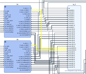
源文件:transport_ADC12DJxx00.v
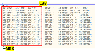
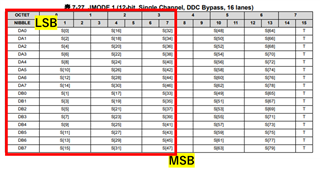
   // Bit pattern for JMODE1. Please refer ADC12DJxx00 datasheet for more details
   // Bit packing format is same for both JMODE1 and JMODE3. Please view this verilog file in notepad++ to have proper alignment of the table shown below
   // On 3rd link clock, 40 samples from first half of first frame is sent out- [S0, S1,.., S39] with S0 as MSB in rx_dataout signal
   // On the 4th link clock, 40 samples from second half of first frame is sent out- [S40, S41,.., S79] with S40 as MSB in rx_dataout signal
   // On the 5th link clock, 40 samples from the first half of second frame is sent out- [S0, S1, S2, …, S39] with S0 as MSB in rx_dataout signal and the sequence repeats
   // Out samples are delayed by 3 link clocks, due to internal registering


   /*
	s0	31:20	s16	19:8	s32	7:0			31:28		s48	27:16	s64	15:4	3:0
	s2	63:52	s18	51:40	s34	39:32		63:60		s50	59:48	s66	47:36	35:32
	s4	95:84	s20	83:72	s36	71:64		95:92		s52	91:80	s68	79:68	67:64
	s6	127:116	s22	115:104	s38	103:96		127:124		s54	123:112	s70	111:100	99:96
	s8	159:148	s24	147:136	s40	135:128		159:156		s56	155:144	s72	143:132	131:128
	s10	191:180	s26	179:168	s42	167:160		191:188		s58	187:176	s74	175:164	163:160
	s12	223:212	s28	211:200	s44	199:192		223:220		s60	219:208	s76	207:196	195:192
	s14	255:244	s30	243:232	s46	231:224		255:252		s62	251:240	s78	239:228	227:224
	s1	287:276 s17	275:264 s33	263:256		287:284		s49	283:272	s65	271:260	259:256
	s3	319:308	s19	307:296	s35	295:288		319:316		s51	315:304	s67	303:290	291:288
	s5	351:340	s21	339:328	s37 327:320		351:348		s53	347:336	s69	335:324	323:320
	s7	383:372	s23	371:360	s39	359:352		383:380		s55	379:368	s71	367:356	355:352
	s9	415:404	s25	403:392	s41	391:384		415:412		s57	411:400	s73	399:388	387:384
	s11	447:436	s27	435:424	s43	423:416		447:444		s59 443:432	s75	431:420	419:416
	s13	479:468	s29	467:456 s45	455:448		479:476		s61	475:464	s77	463:452	451:448
	s15	511:500	s31	499:488	s47	487:480		511:508		s63	507:496	s79	495:482	483:480
	*/
根据注释,LSB=>S32、MSB=>S15
但是、ADC12DJ5200RF 数据表指出、数据首先发送 MSB。
所以我认为 MSB 和 LSB 将如下所示。
LSB=>S0、MSB=>S47
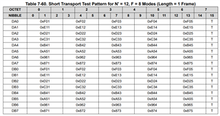
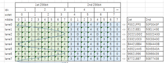
例如、我认为短传输层的测试模式将如下图所示。
应该怎么做?
我很抱歉我没有说明清楚。
此致、
竹尾市