This thread has been locked.

If you have a related question, please click the "Ask a related question" button in the top right corner. The newly created question will be automatically linked to this question.

[参考译文] LMH1219:LMH1219

Guru**** 657930 points
Other Parts Discussed in Thread: LMH1218, LMH1219
请注意,本文内容源自机器翻译,可能存在语法或其它翻译错误,仅供参考。如需获取准确内容,请参阅链接中的英语原文或自行翻译。

https://e2e.ti.com/support/interface-group/interface/f/interface-forum/1276185/lmh1219-lmh1219

器件型号:LMH1219
主题中讨论的其他器件:LMH1218

大家好!

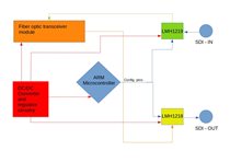
我将使用 LMH1219作为 TX、LMH1218作为 RX 来开发光纤到 SDI 双向转换器。

我在《编程指南》的指引下编写了代码、但 LMH1218未显示已接收到 LMH1219的映像。

我想知道我是否可以发送与器件设置相关的代码片段、以便您可以对其进行分析、如果存在错误、您可以帮助我更正它

我可以发送吗?

谢谢

马塞洛

阿尔法辛

  • 请注意,本文内容源自机器翻译,可能存在语法或其它翻译错误,仅供参考。如需获取准确内容,请参阅链接中的英语原文或自行翻译。

    尊敬的 Marcelo:

    您可以发送此代码片段。 还请包含一个方框图。

    此致、Nasser

  • 请注意,本文内容源自机器翻译,可能存在语法或其它翻译错误,仅供参考。如需获取准确内容,请参阅链接中的英语原文或自行翻译。

    尊敬的 Nasser:

    感谢您在代码和方框图上方接收我的"查询"。

    代码:

    void Config_Chip_TX()//Rotina de configuração do chip conversor de fibra para SDI como TX
    {
    	//Para operacao de escrita devemos colocar 0 antes do endereco
    	//Para operacao de leitura devemos colocar 1 antes do endereco
    
    	//---------Configuracoes------------------------------------------------
    		/*habilita a pagina do registrador CTLE/CDR
    		HAL_GPIO_WritePin(GPIOA, CS_1_Pin, 0);
    		operacao_tx = 0x00;
    		endereco_tx = 0xFF;
    		dado_tx	 	= 0x04;
    		mascara_tx	= 0x07;
    		comando_tx = operacao_tx+endereco_tx+dado_tx+mascara_tx;
    		HAL_SPI_Transmit(&hspi1, &comando_tx, 1, 100);
    		HAL_GPIO_WritePin(GPIOA, CS_1_Pin, 1);
    		HAL_Delay(100);*/
    
    		//habilita a pagina do registrador CableEQ/Drivers
    		HAL_GPIO_WritePin(GPIOA, CS_1_Pin, 0);
    		operacao_tx = 0x00;
    		endereco_tx = 0xFF;
    		dado_tx	 	= 0x05;
    		mascara_tx	= 0x07;
    		comando_tx = operacao_tx+endereco_tx+dado_tx+mascara_tx;
    		HAL_SPI_Transmit(&hspi1, &comando_tx, 1, 100);
    		HAL_GPIO_WritePin(GPIOA, CS_1_Pin, 1);
    		HAL_Delay(100);
    
    		//habilita IN0 para OUT0
    		HAL_GPIO_WritePin(GPIOA, CS_1_Pin, 0);
    		operacao_tx = 0x00;
    		endereco_tx = 0x31;
    		dado_tx     = 0x20;
    		mascara_tx  = 0x30;
    		comando_tx  = operacao_tx+endereco_tx+dado_tx+mascara_tx;
    		HAL_SPI_Transmit(&hspi1, &comando_tx, 1, 100);
    		HAL_GPIO_WritePin(GPIOA, CS_1_Pin, 1);
    		HAL_Delay(100);
    
    		//habilita a pagina do registrador CableEQ/Drivers
    		HAL_GPIO_WritePin(GPIOA, CS_1_Pin, 0);
    		operacao_tx = 0x00;
    		endereco_tx = 0xFF;
    		dado_tx	 	= 0x05;
    		mascara_tx	= 0x07;
    		comando_tx = operacao_tx+endereco_tx+dado_tx+mascara_tx;
    		HAL_SPI_Transmit(&hspi1, &comando_tx, 1, 100);
    		HAL_GPIO_WritePin(GPIOA, CS_1_Pin, 1);
    		HAL_Delay(100);
    
    		//habilita controle independente das saidas OUT0 e OUT1
    		HAL_GPIO_WritePin(GPIOA, CS_1_Pin, 0);
    		operacao_tx = 0x00;
    		endereco_tx = 0x09;
    		dado_tx     = 0x20;
    		mascara_tx  = 0x20;
    		comando_tx  = operacao_tx+endereco_tx+dado_tx+mascara_tx;
    		HAL_SPI_Transmit(&hspi1, &comando_tx, 1, 100);
    		HAL_GPIO_WritePin(GPIOA, CS_1_Pin, 1);
    		HAL_Delay(100);
    
    		//habilita a pagina do registrador CableEQ/Drivers
    		HAL_GPIO_WritePin(GPIOA, CS_1_Pin, 0);
    		operacao_tx = 0x00;
    		endereco_tx = 0xFF;
    		dado_tx	 	= 0x05;
    		mascara_tx	= 0x07;
    		comando_tx = operacao_tx+endereco_tx+dado_tx+mascara_tx;
    		HAL_SPI_Transmit(&hspi1, &comando_tx, 1, 100);
    		HAL_GPIO_WritePin(GPIOA, CS_1_Pin, 1);
    		HAL_Delay(100);
    
    		//habilita reclocker
    		HAL_GPIO_WritePin(GPIOA, CS_1_Pin, 0);
    		operacao_tx = 0x00;
    		endereco_tx = 0x1C;
    		dado_tx     = 0x80;
    		mascara_tx  = 0xE0;
    		comando_tx  = operacao_tx+endereco_tx+dado_tx+mascara_tx;
    		HAL_SPI_Transmit(&hspi1, &comando_tx, 1, 100);
    		HAL_GPIO_WritePin(GPIOA, CS_1_Pin, 1);
    		HAL_Delay(100);
    
    
    }
    
    void Config_Chip_RX()
    {
    	//Para operacao de escrita devemos colocar 0 antes do endereco
    	//Para operacao de leitura devemos colocar 1 antes do endereco
    
    	//---------Configura para modo CD------------------------------------------------
    	//acesso ao regustrador da pagina compartilhada
    	HAL_GPIO_WritePin(GPIOA, CS_2_Pin, 0);
    	operacao_rx = 0x00;
    	endereco_rx = 0xFF;
    	dado_rx     = 0x04;
    	mascara_rx  = 0x07;
    	comando_rx = operacao_rx+endereco_rx+dado_rx+mascara_rx;
    	HAL_SPI_Transmit(&hspi1, &comando_rx, 1, 100);
    	HAL_GPIO_WritePin(GPIOA, CS_2_Pin, 1);
    	HAL_Delay(100);
    
    	//seleciona IN0 para OUT0
    	HAL_GPIO_WritePin(GPIOA, CS_2_Pin, 0);
    	operacao_rx = 0x00;
    	endereco_rx = 0x31;
    	dado_rx     = 0x01;
    	mascara_rx  = 0x03;
    	comando_rx = operacao_rx+endereco_rx+dado_rx+mascara_rx;
    	HAL_SPI_Transmit(&hspi1, &comando_rx, 1, 100);
    	HAL_GPIO_WritePin(GPIOA, CS_2_Pin, 1);
    	HAL_Delay(100);
    
    	//acesso ao regustrador da pagina compartilhada
    	HAL_GPIO_WritePin(GPIOA, CS_2_Pin, 0);
    	operacao_rx = 0x00;
    	endereco_rx = 0xFF;
    	dado_rx     = 0x04;
    	mascara_rx  = 0x07;
    	comando_rx = operacao_rx+endereco_rx+dado_rx+mascara_rx;
    	HAL_SPI_Transmit(&hspi1, &comando_rx, 1, 100);
    	HAL_GPIO_WritePin(GPIOA, CS_2_Pin, 1);
    	HAL_Delay(100);
    
    	//detecção de operação normal em IN0
    	HAL_GPIO_WritePin(GPIOA, CS_2_Pin, 0);
    	operacao_rx = 0x00;
    	endereco_rx = 0x14;
    	dado_rx     = 0x00;
    	mascara_rx  = 0xC0;
    	comando_rx = operacao_rx+endereco_rx+dado_rx+mascara_rx;
    	HAL_SPI_Transmit(&hspi1, &comando_rx, 1, 100);
    	HAL_GPIO_WritePin(GPIOA, CS_2_Pin, 1);
    	HAL_Delay(100);
    
    	//acesso ao regustrador da pagina compartilhada
    	HAL_GPIO_WritePin(GPIOA, CS_2_Pin, 0);
    	operacao_rx = 0x00;
    	endereco_rx = 0xFF;
    	dado_rx     = 0x04;
    	mascara_rx  = 0x07;
    	comando_rx = operacao_rx+endereco_rx+dado_rx+mascara_rx;
    	HAL_SPI_Transmit(&hspi1, &comando_rx, 1, 100);
    	HAL_GPIO_WritePin(GPIOA, CS_2_Pin, 1);
    	HAL_Delay(100);
    
    	//OUT0 reclocked
    	HAL_GPIO_WritePin(GPIOA, CS_2_Pin, 0);
    	operacao_rx = 0x00;
    	endereco_rx = 0x1C;
    	dado_rx     = 0x08;
    	mascara_rx  = 0x0C;
    	comando_rx = operacao_rx+endereco_rx+dado_rx+mascara_rx;
    	HAL_SPI_Transmit(&hspi1, &comando_rx, 1, 100);
    	HAL_GPIO_WritePin(GPIOA, CS_2_Pin, 1);
    	HAL_Delay(100);


    }
    

    此致、Marcelo

  • 请注意,本文内容源自机器翻译,可能存在语法或其它翻译错误,仅供参考。如需获取准确内容,请参阅链接中的英语原文或自行翻译。

    尊敬的 Marcelo:

    A)。 请允许我确保我理解该方框图。 LMH1219具有两个100欧姆高速输出。 我们为什么不使用其中一个输出并向 LMH1218 100欧姆高速输入提供这些输出? 或者、LMH1218高速输入来自光学模块接收器?

    B)。 LMH1219是否显示锁定指示? 上面的寄存器似乎没有显示这一点?

    c)> LMH1218相同。 请查看 LMH1218编程指南并让我们了解 CDR.0x03内容。

    d)。 您是否可以使用 LMH1219 GUI? 只要您使用 SMBus 接口、就可以执行此操作。 GUI 根据需要设置器件。 此外、GUI 顶层还为我们提供了 LMH1219和 LMH1218器件的状态。

    此致、Nasser  

  • 请注意,本文内容源自机器翻译,可能存在语法或其它翻译错误,仅供参考。如需获取准确内容,请参阅链接中的英语原文或自行翻译。

    尊敬的 Nasser:

    我将尝试回答您的问题...

    A)例如、LMH1219将接收由摄像头发送的 SDI 信号、然后传输到光纤收发器、以便发送到另一个设备视频。 但是、LMH1218将通过光纤收发器接收另一个信号、并会收到另一个设备视频、然后将该信号传输到 SDI 第3个设备的视频。 请注意,不同的信号到不同的 pourposes.

    b)是的、LMH1219在输入引脚中有信号时会显示锁定指示。

    C) LMH1218在有或没有要发送的信号时独立保持锁定指示处于全时状态。

    d)不、很遗憾不、因为我将使用原型板来开发固件以配置此器件、更改通信方法会导致此电路板丢失、我需要重新绘制所有项目、并为此项目抽出更多时间。

    此致、Marcelo

  • 请注意,本文内容源自机器翻译,可能存在语法或其它翻译错误,仅供参考。如需获取准确内容,请参阅链接中的英语原文或自行翻译。

    尊敬的 Marcelo:

    希望您做得好、我将协助 Nasser。  

    C) LMH1218可以在有信号或没有信号的情况下随时保持锁定指示。
    • 如何确定锁定指示? 您是否在使用 TI 的 LMH1218 EVM? 如果是、您将能够在绿色 LED D1上看到锁定指示。 否则、使用 SPI 看到它的一种方法是读取寄存器 CDR 0x02、如果结果为5C、则表示您处于锁定状态。
    注意,不同的信号是不同的 pourposes.
    • 您是否在均衡器模式下使用两个 LMH 器件?
    B)是的,当 LMH1219的输入引脚中有信号时,它会显示锁定指示。
    • 如何才能看到锁定指示?

    如需调试代码方面的进一步帮助、请参阅有关 SPI 的这段视频: https://training.ti.com/spi-access-using-fpga-or-asic-using-lmh12xx-12g-sdi-devices

    此致!

    尼克