This thread has been locked.

If you have a related question, please click the "Ask a related question" button in the top right corner. The newly created question will be automatically linked to this question.

[参考译文] SN74LVC2G17-Q1:SC70封装布局

Guru**** 2538930 points


请注意,本文内容源自机器翻译,可能存在语法或其它翻译错误,仅供参考。如需获取准确内容,请参阅链接中的英语原文或自行翻译。

https://e2e.ti.com/support/logic-group/logic/f/logic-forum/934566/sn74lvc2g17-q1-sc70-package-layout

器件型号:SN74LVC2G17-Q1

大家好、

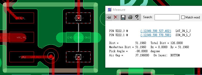
根据数据表,封装为2.2mm×1.3mm,而不是1.9mm×1.33。 您能告诉我这种差异是否很重要?

12424.402-12349.598=74.804mil=1.9mm

578.598-527.402=51.196mil=1.3mm

此致、

罗伊

  • 请注意,本文内容源自机器翻译,可能存在语法或其它翻译错误,仅供参考。如需获取准确内容,请参阅链接中的英语原文或自行翻译。

    根据数据表、封装尺寸可以介于1.85mm×1.10mm 和2.15mm×1.40mm 之间。

    引脚间距为0.65mm、因此最外侧两个焊盘中心之间的距离应恰好为1.3mm。

    引脚的外边缘可以在1.80 mm 和2.40 mm 之间任意位置。 焊盘中心距2.2 mm、因为焊盘比引脚大、可实现更好的焊接。