

请注意,本文内容源自机器翻译,可能存在语法或其它翻译错误,仅供参考。如需获取准确内容,请参阅链接中的英语原文或自行翻译。
部件号:MSP430F5132 各位专家,您好!
我的ADC初始化是否不正确? 无论我尝试什么,我都无法清除中断标志。 读取MEM0不会清除IFG0标志,设置ADC10IFG =0不会清除。
当我越过线125时,所有ADC10IFG立即设置为1,尽管没有ADC读数:

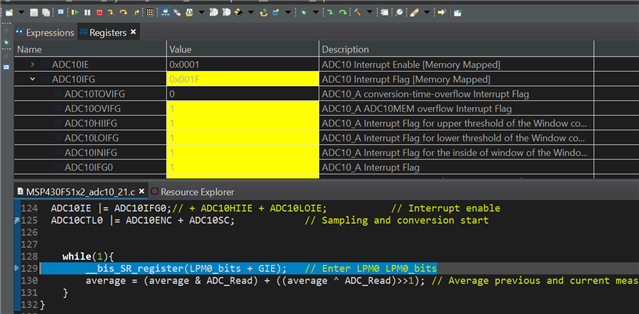
在中断向量内,我无法清除标志:


/* --COPYRIGHT--,BSD_EX
 * Copyright (c) 2012, Texas Instruments Incorporated
 * All rights reserved.
 *
 * Redistribution and use in source and binary forms, with or without
 * modification, are permitted provided that the following conditions
 * are met:
 *
 * *  Redistributions of source code must retain the above copyright
 *    notice, this list of conditions and the following disclaimer.
 *
 * *  Redistributions in binary form must reproduce the above copyright
 *    notice, this list of conditions and the following disclaimer in the
 *    documentation and/or other materials provided with the distribution.
 *
 * *  Neither the name of Texas Instruments Incorporated nor the names of
 *    its contributors may be used to endorse or promote products derived
 *    from this software without specific prior written permission.
 *
 * THIS SOFTWARE IS PROVIDED BY THE COPYRIGHT HOLDERS AND CONTRIBUTORS "AS IS"
 * AND ANY EXPRESS OR IMPLIED WARRANTIES, INCLUDING, BUT NOT LIMITED TO,
 * THE IMPLIED WARRANTIES OF MERCHANTABILITY AND FITNESS FOR A PARTICULAR
 * PURPOSE ARE DISCLAIMED. IN NO EVENT SHALL THE COPYRIGHT OWNER OR
 * CONTRIBUTORS BE LIABLE FOR ANY DIRECT, INDIRECT, INCIDENTAL, SPECIAL,
 * EXEMPLARY, OR CONSEQUENTIAL DAMAGES (INCLUDING, BUT NOT LIMITED TO,
 * PROCUREMENT OF SUBSTITUTE GOODS OR SERVICES; LOSS OF USE, DATA, OR PROFITS;
 * OR BUSINESS INTERRUPTION) HOWEVER CAUSED AND ON ANY THEORY OF LIABILITY,
 * WHETHER IN CONTRACT, STRICT LIABILITY, OR TORT (INCLUDING NEGLIGENCE OR
 * OTHERWISE) ARISING IN ANY WAY OUT OF THE USE OF THIS SOFTWARE,
 * EVEN IF ADVISED OF THE POSSIBILITY OF SUCH DAMAGE.
 *
 *******************************************************************************
 *
 *                       MSP430 CODE EXAMPLE DISCLAIMER
 *
 * MSP430 code examples are self-contained low-level programs that typically
 * demonstrate a single peripheral function or device feature in a highly
 * concise manner. For this the code may rely on the device's power-on default
 * register values and settings such as the clock configuration and care must
 * be taken when combining code from several examples to avoid potential side
 * effects. Also see www.ti.com/grace for a GUI- and www.ti.com/msp430ware
 * for an API functional library-approach to peripheral configuration.
 *
 * --/COPYRIGHT--*/
//******************************************************************************
//  MSP430F51x2 Demo - ADC10, Window Comparator, 2.5V Timer trigger, DCO
//
//  Description; A1 is sampled in every 1s using the TA0.1 trigger in single
//  ch/conversion mode. Window comparator is used to generate interrupts to
//  indicate when the input voltage goes above the High_Threshold or below the
//  Low_Threshold or is inbetween the high and low thresholds. TimerD0 is used
//  as an interval timer used to control the LED at P1.0 to toggle slow/fast
//  or turn off according to the ADC10 Hi/Lo/IN interupts.
//  ADC10 is configured in pulse sample mode and is triggered by the TA0.1
//
//               MSP430F51x2
//            -----------------
//        /|\|              XIN|-
//         | |                 | 32kHz
//         --|RST          XOUT|-
//           |                 |
//       >---|P1.1/A1     P1.0 |--> LED
//           |             P3.6|--> TA0.1 (ADC trigger signal)
//
//  Eason Zhou
//  Texas Instruments Inc.
//  January 2020
//  Built with CCS v9.2.0 and IAR Embedded Workbench Version: 7.12.1
//******************************************************************************
#include <msp430.h>

#define High_Threshold 100 //TODO test to determine
#define Low_Threshold 50
#define ARRAY_SIZE 32

unsigned int SlowToggle_Period = 20000-1;
unsigned int FastToggle_Period = 1000-1;

unsigned int ADC_Read, index = 0;
unsigned int average = 0;               // Average of most recent and previous measurement
unsigned int ADC_Result[ARRAY_SIZE];

int main(void)
{
  WDTCTL = WDTPW + WDTHOLD;                  // Stop WDT

  PMAPPWD = 0x02D52;      // Enable Write-access to modify port mapping registers
  PMAPCTL = PMAPRECFG;    // Allow reconfiguration during runtime
  P1MAP1 |= PM_ANALOG;    // Modify all PxMAPy registers.
  PMAPPWD = 0;            // Disable Write-Access to modify port mapping registers by writing incorrect key
  P1SEL|=BIT1;            // setting the port mapping register PxMAPy to PM_ANALOG together with PxSEL.y=1 when applying analog signals.

  // Configure ADC10;
  ADC10CTL0 = ADC10SHT_2 + ADC10ON + ADC10MSC;
                                              // (ADC10ON) enable ADC10
                                              // (SHTx) clk cycles per sample period
                                              // (MSC) completion of one sample triggers next sample

  ADC10CTL1 = ADC10SHP + ADC10CONSEQ_2 + ADC10SHS_0;  // (SHP) pulse sample mode
                                                      // (SHS) triggered sample with ADC10SC
                                                      // (CONSEQ) repeat-single-channel mode 27.2.7.3


  ADC10CTL2 = ADC10RES;                     // 10-bit conversion results
  ADC10MCTL0 = ADC10INCH_1 + ADC10SREF_1;   // (REF_x) V+ = Vref+, V- = AVSS
                                            // (INCH_x) Read ch Ax (P1.x)

  ADC10HI = High_Threshold;                 // Window Comparator Hi-threshold
  ADC10LO = Low_Threshold;                  // Window Comparator Low-threshold

 // Configure internal reference
  while(REFCTL0 & REFGENBUSY);              // If ref generator busy, WAIT
  REFCTL0 |= REFVSEL_0+REFON;               // (VSEL_x) Select internal ref = 2V
                                            // This sets max FSR for ADC10 per ADC10REF
                                            // (REFON) Internal Reference ON
  __delay_cycles(75);                       // Delay (~75us) for Ref to settle


  P1DIR |= BIT0;                            // Set P1.0 output direction
                                            // TODO will this still allow ADC A0 reading?
  P1OUT &= ~BIT0;                           // Clear P1.0


  ADC10IE |= ADC10IFG0 + ADC10HIIE + ADC10LOIE;           // Interrupt enable
  ADC10CTL0 |= ADC10ENC + ADC10SC;            // Sampling and conversion start


    while(1){
        __bis_SR_register(LPM0_bits + GIE);   // Enter LPM0 LPM0_bits
        average = (average & ADC_Read) + ((average ^ ADC_Read)>>1); // Average previous and current measurements
    }
}

// ADC10 interrupt service routine
#if defined(__TI_COMPILER_VERSION__) || defined(__IAR_SYSTEMS_ICC__)
#pragma vector=ADC10_VECTOR
__interrupt void ADC10_ISR(void)
#elif defined(__GNUC__)
void __attribute__ ((interrupt(ADC10_VECTOR))) ADC10_ISR (void)
#else
#error Compiler not supported!
#endif
{
  switch(__even_in_range(ADC10IV,12))
  {
    case  0: break;                         // No interrupt
    case  2: break;                         // conversion result overflow
    case  4: break;                         // conversion time overflow
    case  6:                                // ADC10HI
        ADC10IFG &= ~ADC10HIIFG;            // Clear interrupt flag
        P1OUT = BIT0;                       // Turn on LED
        break;
    case  8:                                 // ADC10LO
        ADC10IFG &= ~ADC10LOIFG;             // Clear interrupt flag
        P1OUT &= ~BIT0;
        break;
    case 10: break;
    case 12:                                // ADC10IFG0 set when ADC10 conversion is completed
        ADC10IFG &= ~ADC10IFG0;                    // clear interrupt flag TODO delete
        ADC_Read = ADC10MEM0;                        // Read ADC10MEM0 clears IFG0 flag
        __bic_SR_register_on_exit(LPM0_bits + GIE);  // Exit LPM0 on return to main

        break;

    default: break;
  }
}
