请注意,本文内容源自机器翻译,可能存在语法或其它翻译错误,仅供参考。如需获取准确内容,请参阅链接中的英语原文或自行翻译。
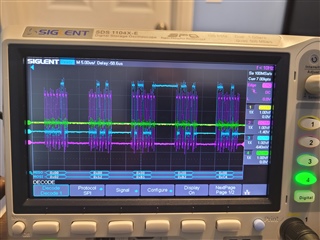
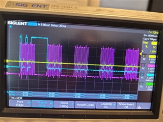
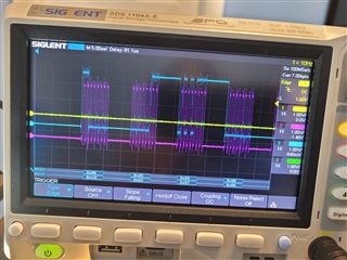
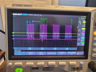
器件型号:LP-MSP430FR2476 使用 MSP430 SPI 和连接到一个 MAX17853的 MAX17841 (表10)、我能够获得对菊花链初始化序列的正确响应。 唤醒和 hello 所有事务在 MISO 线路上接收正确的响应,我得到返回为0x001的器件地址。 这与 Maxim 评估 GUI 相同。 这些 MSP430 SPI 响应已在示波器上捕获。
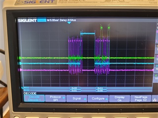
现在、我需要使 MAX17841的表11正常工作。 我发送了事务1、2和3 (WriteAll_transactions[0]= 0xc0; WriteAll_transactions[1]。Data[0]= 0xb0;WriteAll_transactions[2]。Data[0]= 0x01;)、但我没有得到0x12的接收。 相反、我得到0x11 (有时为0x21)、这意味着存在 RX_Overflow_Status 或存在未读数据。 我不明白这是为什么。 在表10中的事务中、命令0xC0和0xB0工作正常。 使用评估 GUI、表11工作正常。 因此、MSP430握手会丢失一些东西。 我感谢任何指示。 我已将当前文件附加到此帖子。
我尝试从 WriteAll_transactions [0]中包含和删除 PEC 字节、但从器件响应没有任何差异。
#include <stdio.h>
#include <stdlib.h>
#include <stdint.h>
#include <string.h>
#include <driverlib.h>
#include <intrinsics.h>
#include <msp430.h>
#include "clock~.h" // Clock configurations
#define UART_TRANSMIT_BUFFER_LENGTH 76
#define UART_TXD_PORT GPIO_PORT_P1
#define UART_TXD_PIN GPIO_PIN4
#define UART_RXD_PORT GPIO_PORT_P1
#define UART_RXD_PIN GPIO_PIN5
#define UART_SELECT_FUNCTION GPIO_PRIMARY_MODULE_FUNCTION
#define SPI_MOSI_PORT GPIO_PORT_P2
#define SPI_MOSI_PIN GPIO_PIN6
#define SPI_MISO_PORT GPIO_PORT_P2
#define SPI_MISO_PIN GPIO_PIN5
#define SPI_CLK_PORT GPIO_PORT_P2
#define SPI_CLK_PIN GPIO_PIN4
#define SPI_SELECT_FUNCTION GPIO_PRIMARY_MODULE_FUNCTION
typedef struct {
uint8_t Len;
uint8_t Data[10];
} spi_MaximTrans_t;
static uint8_t RXData[8] = {0}; //SPI receive byte
/**
* Initialize system clocks
*/
static void init_clock(void) {
// Configure one FRAM waitstate as required by the device datasheet for MCLK
// operation beyond 8MHz _before_ configuring the clock system.
FRAMCtl_configureWaitStateControl(FRAMCTL_ACCESS_TIME_CYCLES_1);
//Set DCO FLL reference = REFO
CS_initClockSignal(CS_FLLREF, CS_REFOCLK_SELECT, CS_CLOCK_DIVIDER_1);
//Set ACLK = REFO
CS_initClockSignal(CS_ACLK, CS_REFOCLK_SELECT, CS_CLOCK_DIVIDER_1);
CS_initFLLParam param = {0};
//Set Ratio/Desired MCLK Frequency, initialize DCO, save trim values
CS_initFLLCalculateTrim(CS_MCLK_DESIRED_FREQUENCY_IN_KHZ, CS_MCLK_FLLREF_RATIO, ¶m);
//Set MCLK = REFO
CS_initClockSignal(CS_MCLK, CS_REFOCLK_SELECT, CS_CLOCK_DIVIDER_1);
//Set SMCLK = DCO
CS_initClockSignal(CS_SMCLK, CS_DCOCLKDIV_SELECT, CS_CLOCK_DIVIDER_1);
//Clear all OSC fault flag
CS_clearAllOscFlagsWithTimeout(1000);
}
/**
* Initialize all of the IO pins per their configuration
*/
static void init_gpio(void) {
// Set all GPIO pins to output low to prevent floating input and reduce power consumption
GPIO_setOutputLowOnPin(GPIO_PORT_P1, GPIO_PIN_ALL8);
GPIO_setOutputLowOnPin(GPIO_PORT_P2, GPIO_PIN_ALL8);
GPIO_setOutputLowOnPin(GPIO_PORT_P3, GPIO_PIN_ALL8);
GPIO_setOutputLowOnPin(GPIO_PORT_P4, GPIO_PIN_ALL8);
GPIO_setOutputLowOnPin(GPIO_PORT_P5, GPIO_PIN_ALL8);
GPIO_setOutputLowOnPin(GPIO_PORT_P6, GPIO_PIN0 | GPIO_PIN1 | GPIO_PIN2);
GPIO_setAsOutputPin( GPIO_PORT_P1, GPIO_PIN_ALL8);
GPIO_setAsOutputPin( GPIO_PORT_P2, GPIO_PIN_ALL8);
GPIO_setAsOutputPin( GPIO_PORT_P3, GPIO_PIN_ALL8);
GPIO_setAsOutputPin( GPIO_PORT_P4, GPIO_PIN_ALL8);
GPIO_setAsOutputPin( GPIO_PORT_P5, GPIO_PIN_ALL8);
GPIO_setAsOutputPin( GPIO_PORT_P6, GPIO_PIN0 | GPIO_PIN1 | GPIO_PIN2);
}
/*
* Initialize the SPI peripheral on EUSCI A1
*/
void init_spi_peripheral()
{
GPIO_setAsPeripheralModuleFunctionOutputPin(SPI_MOSI_PORT, SPI_MOSI_PIN, SPI_SELECT_FUNCTION);
GPIO_setAsPeripheralModuleFunctionInputPin(SPI_MISO_PORT, SPI_MISO_PIN, SPI_SELECT_FUNCTION);
GPIO_setAsPeripheralModuleFunctionOutputPin(SPI_CLK_PORT, SPI_CLK_PIN, SPI_SELECT_FUNCTION);
//Initialize Master
EUSCI_A_SPI_initMasterParam param = {0};
param.selectClockSource = EUSCI_A_SPI_CLOCKSOURCE_SMCLK;
param.clockSourceFrequency = CS_getSMCLK();
param.desiredSpiClock = 1000000;
param.msbFirst = UCMSB;
param.clockPhase = EUSCI_A_SPI_PHASE_DATA_CAPTURED_ONFIRST_CHANGED_ON_NEXT;
param.clockPolarity = EUSCI_A_SPI_CLOCKPOLARITY_INACTIVITY_LOW;
param.spiMode = EUSCI_A_SPI_3PIN;
EUSCI_A_SPI_initMaster(EUSCI_A1_BASE, ¶m);
EUSCI_A_SPI_enable(EUSCI_A1_BASE);
}
void init_wd_bms_uart(void)
{
// Configure UART @38400 baud (EUSCI/16MHz)
// software-dl.ti.com/.../index.html
// Configure UCA0TXD and UCA0RXD
GPIO_setAsPeripheralModuleFunctionOutputPin(UART_TXD_PORT, UART_TXD_PIN, UART_SELECT_FUNCTION);
GPIO_setAsPeripheralModuleFunctionInputPin(UART_RXD_PORT, UART_RXD_PIN, UART_SELECT_FUNCTION);
EUSCI_A_UART_initParam param = {
.clockPrescalar = 26, .firstModReg = 0, .secondModReg = 214,
.selectClockSource = EUSCI_A_UART_CLOCKSOURCE_SMCLK,
.parity = EUSCI_A_UART_NO_PARITY,
.msborLsbFirst = EUSCI_A_UART_LSB_FIRST,
.numberofStopBits = EUSCI_A_UART_ONE_STOP_BIT,
.uartMode = EUSCI_A_UART_MODE,
.overSampling = EUSCI_A_UART_OVERSAMPLING_BAUDRATE_GENERATION
};
if(STATUS_FAIL == EUSCI_A_UART_init(EUSCI_A0_BASE, ¶m))
{
return;
}
EUSCI_A_UART_enable(EUSCI_A0_BASE);
}
/**
* UART_Transmit_String()
* Prints a null terminated string on the UART
* @param str null terminated string
*/
void UART_Transmit_String(const char *str)
{
int i = 0;
for(i = 0; i < UART_TRANSMIT_BUFFER_LENGTH; i++)
{
if (str[i] != '\0')
{
while (EUSCI_A_UART_queryStatusFlags(EUSCI_A0_BASE, EUSCI_A_UART_BUSY));
EUSCI_A_UART_transmitData(EUSCI_A0_BASE, str[i]);
}
else
{
break;
}
}
}
void SetUpDCInitTransactions(spi_MaximTrans_t DCInit_transactions[]){
//Enable keep alive mode
DCInit_transactions[0].Len = 2;
DCInit_transactions[0].Data[0] = 0x10;
DCInit_transactions[0].Data[1] = 0x5;
//Read Back Transaction byte
DCInit_transactions[1].Len = 2;
DCInit_transactions[1].Data[0] = 0x11;
DCInit_transactions[1].Data[1] = 0x0;
//Enable Rx Interrupt flags
DCInit_transactions[2].Len = 2;
DCInit_transactions[2].Data[0] = 0x4;
DCInit_transactions[2].Data[1] = 0x89;
//No Receive
//Read Back Transaction byte
DCInit_transactions[3].Len = 2;
DCInit_transactions[3].Data[0] = 0x5;
DCInit_transactions[3].Data[1] = 0x0;
//Clear receive buffer
DCInit_transactions[4].Len = 1;
DCInit_transactions[4].Data[0] = 0xe0;
//No Receive
//Wakeup UART slave devices
DCInit_transactions[5].Len = 2;
DCInit_transactions[5].Data[0] = 0x0e;
DCInit_transactions[5].Data[1] = 0x30;
//No Receive
//Read Back Transaction byte
DCInit_transactions[6].Len = 2;
DCInit_transactions[6].Data[0] = 0x0f;
DCInit_transactions[6].Data[1] = 0x0;
//No Receive
//2ms delay for each slave to wake up
//Wait for all UART slave devices to wake up
DCInit_transactions[7].Len = 2;
DCInit_transactions[7].Data[0] = 0x01;
DCInit_transactions[7].Data[1] = 0x0;
//Receive of 0x21 expected
//End of UART slave device wake-up period
DCInit_transactions[8].Len = 2;
DCInit_transactions[8].Data[0] = 0x0e;
DCInit_transactions[8].Data[1] = 0x10;
//Read Back Transaction byte
DCInit_transactions[9].Len = 2;
DCInit_transactions[9].Data[0] = 0x0f;
DCInit_transactions[9].Data[1] = 0x0;
//No Receive
//2ms delay for each slave to report null message
//Wait for null message to be received
DCInit_transactions[10].Len = 2;
DCInit_transactions[10].Data[0] = 0x01;
DCInit_transactions[10].Data[1] = 0x0;
//Receive 0x10 or 0x12
//Clear transmit buffer
DCInit_transactions[11].Len = 1;
DCInit_transactions[11].Data[0] = 0x20;
//No Receive
//Clear receive buffer
DCInit_transactions[12].Len = 1;
DCInit_transactions[12].Data[0] = 0xe0;
//No Receive
//Load the HELLOALL command sequence into the load queue
DCInit_transactions[13].Len = 5;
DCInit_transactions[13].Data[0] = 0xc0;
DCInit_transactions[13].Data[1] = 0x03; //message length
DCInit_transactions[13].Data[2] = 0x57; //HELLOALL command byte
DCInit_transactions[13].Data[3] = 0x0; //Register address (0x00)
DCInit_transactions[13].Data[4] = 0x0; //Initialization address of HELLOALL
//Verify contents of the load queue
DCInit_transactions[14].Len = 5;
DCInit_transactions[14].Data[0] = 0xc1;
DCInit_transactions[14].Data[1] = 0x0;
DCInit_transactions[14].Data[2] = 0x0;
DCInit_transactions[14].Data[3] = 0x0;
DCInit_transactions[14].Data[4] = 0x0;
//Transmit HELLOALL sequence
DCInit_transactions[15].Len = 1;
DCInit_transactions[15].Data[0] = 0xb0;
//No Receive
//2ms delay for each slave to respond
//Poll RX_Stop_Status Bit
DCInit_transactions[16].Len = 2;
DCInit_transactions[16].Data[0] = 0x01;
DCInit_transactions[16].Data[1] = 0x0;
//Receive 0x12
//Service receive buffer. Read the HELLOALL message that propagated through the daisy chain
//and was returned back to the ASCI.The host should verify the device count
DCInit_transactions[17].Len = 4;
DCInit_transactions[17].Data[0] = 0x93;
DCInit_transactions[17].Data[1] = 0x0;
DCInit_transactions[17].Data[2] = 0x0;
DCInit_transactions[17].Data[3] = 0x0;
//Check for receive buffer errors
DCInit_transactions[18].Len = 0x09;
DCInit_transactions[18].Data[0] = 0x0;
}
SPI_Send(spi_MaximTrans_t Transmit[], uint8_t index){
uint8_t SPI_TX_index = 0; //byte count in transaction
GPIO_setOutputLowOnPin(GPIO_PORT_P3, GPIO_PIN1); //Maxim chip select low
__delay_cycles(1000); //idle time between CS change
for(SPI_TX_index = 0; SPI_TX_index < Transmit[index].Len; SPI_TX_index++){
while(!(UCA1IFG & UCTXIFG));
UCA1TXBUF = Transmit[index].Data[SPI_TX_index];
while (!(UCA1IFG & UCRXIFG));
RXData[SPI_TX_index] = UCA1RXBUF;
}
return;
}
/**
* main.c
*/
int main(void)
{
static uint8_t TXData = 0; //transaction count
static spi_MaximTrans_t DCInit_transactions[19];
static spi_MaximTrans_t WriteAll_transactions[3];
static spi_MaximTrans_t ReadAll_transactions[3];
static uint8_t noReceive = 0;
static uint8_t noInc = 0;
char buf[76];
WDTCTL = WDTPW | WDTHOLD; // stop watchdog timer
init_clock();
init_gpio(); // Set up IO pins
GPIO_setOutputHighOnPin(GPIO_PORT_P3, GPIO_PIN1); //SPI slave chip select
// Set P1.0 to output direction
GPIO_setAsOutputPin (GPIO_PORT_P1, GPIO_PIN0);
GPIO_setAsInputPinWithPullUpResistor (GPIO_PORT_P4, GPIO_PIN2);
GPIO_enableInterrupt (GPIO_PORT_P4, GPIO_PIN2);
GPIO_selectInterruptEdge (GPIO_PORT_P4, GPIO_PIN2, GPIO_HIGH_TO_LOW_TRANSITION);
GPIO_clearInterrupt (GPIO_PORT_P4, GPIO_PIN2);
GPIO_setAsOutputPin (GPIO_PORT_P6, GPIO_PIN2);
PMM_unlockLPM5();
__enable_interrupt();
SetUpDCInitTransactions(DCInit_transactions);
TXData = 0x0; // Holds transaction number
// Setup peripheral(s) now that gpio and clocks are setup
init_spi_peripheral(); // Init Maxim spi peripheral
init_wd_bms_uart();
GPIO_setOutputHighOnPin (GPIO_PORT_P6, GPIO_PIN2); //SHDNL held high for 4ms to ensure all slaves are powered on
__delay_cycles(32000);
while (TXData < 19){
noInc = 0;
SPI_Send(DCInit_transactions, TXData);
if ((TXData == 6) || (TXData == 9) || (TXData == 15))
__delay_cycles(32000); //wait for slaves to wake up
if (TXData == 7){
if (RXData[DCInit_transactions[7].Len-1] == 0x21){
TXData++;
noReceive = 0;
noInc = 1;
sprintf(buf, "Wake Up status 0x21 received\n\r");
UART_Transmit_String(buf);
}
if (RXData[DCInit_transactions[7].Len-1] != 0x21){
TXData = 7;
noReceive++;
if (noReceive == 3){
sprintf(buf, "Wakeup Error\n\r"); //Need to set a Fault
UART_Transmit_String(buf);
}
}
}
if (TXData == 10){
if ((RXData[DCInit_transactions[10].Len-1] == 0x10) || (RXData[DCInit_transactions[10].Len-1] == 0x12)){
TXData++;
noReceive = 0;
noInc = 1;
sprintf(buf, "Wakeup Successful\n\r");
UART_Transmit_String(buf);
}
else{
TXData = 10;
noReceive++;
if (noReceive == 3){
sprintf(buf, "Wakeup Error: Preamble not received\n\r"); //Need to set a Fault
UART_Transmit_String(buf);
}
}
}
if (TXData == 16){
if ((RXData[DCInit_transactions[16].Len-1] == 0x12)){
TXData++;
noReceive = 0;
noInc = 1;
sprintf(buf, "HELLOALL successful\n\r");
UART_Transmit_String(buf);
}
else{
TXData = 16;
noReceive++;
if (noReceive == 3){
sprintf(buf, "Wakeup Error: Preamble not received\n\r"); //Need to set a Fault
UART_Transmit_String(buf);
}
}
}
if ((noReceive == 0) && !noInc){
TXData++;
}
if (TXData < 19){
GPIO_setOutputHighOnPin(GPIO_PORT_P3, GPIO_PIN1); //Maxim chip select high
__delay_cycles(1000); //idle time between CS change
}
}
GPIO_setOutputHighOnPin(GPIO_PORT_P3, GPIO_PIN1); //Maxim chip select high
__delay_cycles(1000); //idle time between CS change
//Load WRITEALL sequence into the load queue
WriteAll_transactions[0].Len = 7;
WriteAll_transactions[0].Data[0] = 0xc0; //WR_LD_Q_SPI command byte
WriteAll_transactions[0].Data[1] = 5;
WriteAll_transactions[0].Data[2] = 0x02; //WRITEALL
WriteAll_transactions[0].Data[3] = 0x12; //ADDRESS
WriteAll_transactions[0].Data[4] = 0xb1;
WriteAll_transactions[0].Data[5] = 0xb2;
WriteAll_transactions[0].Data[6] = 0Xc4; //PEC byte
// WriteAll_transactions[0].Data[7] = 0x0; //alive counter byte
SPI_Send(WriteAll_transactions, 0);
GPIO_setOutputHighOnPin(GPIO_PORT_P3, GPIO_PIN1); //Maxim chip select high
__delay_cycles(1000); //idle time between CS change
//Start transmitting the WRITEALL sequence from the transmit queue
WriteAll_transactions[1].Len = 1;
WriteAll_transactions[1].Data[0] = 0xb0; //WR_NXT_LD_Q_SPI command byte
SPI_Send(WriteAll_transactions, 1);
__delay_cycles(32000);
GPIO_setOutputHighOnPin(GPIO_PORT_P3, GPIO_PIN1); //Maxim chip select high
__delay_cycles(1000); //idle time between CS change
WriteAll_transactions[2].Len = 2;
WriteAll_transactions[2].Data[0] = 0x01; //Read RX_Status register
WriteAll_transactions[2].Data[1] = 0x0;
noReceive = 1;
while ((noReceive > 0) && (noReceive < 3)){
SPI_Send(WriteAll_transactions, 2);
if (RXData[WriteAll_transactions[2].Len-1] == 0x12){
sprintf(buf, "WRITEALL acknowledged\n\r");
UART_Transmit_String(buf);
noReceive = 0;
}
else{
noReceive++;
GPIO_setOutputHighOnPin(GPIO_PORT_P3, GPIO_PIN1); //Maxim chip select high
__delay_cycles(1000); //idle time between CS change
if (noReceive == 3){
sprintf(buf, "Writeall Error: not acknowledged\n\r"); //Need to set a Fault
UART_Transmit_String(buf);
}
}
}
GPIO_setOutputHighOnPin(GPIO_PORT_P3, GPIO_PIN1); //Maxim chip select high
__delay_cycles(1000); //idle time between CS change
ReadAll_transactions[0].Len = 7;
ReadAll_transactions[0].Data[0] = 0x93;
ReadAll_transactions[0].Data[1] = 0x0;
ReadAll_transactions[0].Data[2] = 0x0;
ReadAll_transactions[0].Data[3] = 0x0;
ReadAll_transactions[0].Data[4] = 0x0;
ReadAll_transactions[0].Data[5] = 0x0;
ReadAll_transactions[0].Data[6] = 0x0;
SPI_Send(ReadAll_transactions, 0);
GPIO_setOutputHighOnPin(GPIO_PORT_P3, GPIO_PIN1); //Maxim chip select high
__delay_cycles(1000); //idle time between CS change
ReadAll_transactions[1].Len = 2;
ReadAll_transactions[1].Data[0] = 0x09;
ReadAll_transactions[1].Data[1] = 0x0;
SPI_Send(ReadAll_transactions, 0);
GPIO_setOutputHighOnPin(GPIO_PORT_P3, GPIO_PIN1); //Maxim chip select high
__delay_cycles(1000); //idle time between CS change
}
//******************************************************************************
//
//This is the PORT2_VECTOR interrupt vector service routine
//
//******************************************************************************
#if defined(__TI_COMPILER_VERSION__) || defined(__IAR_SYSTEMS_ICC__)
#pragma vector=PORT4_VECTOR
__interrupt
#elif defined(__GNUC__)
__attribute__((interrupt(PORT2_VECTOR)))
#endif
void P4_ISR (void)
{
GPIO_clearInterrupt (GPIO_PORT_P4, GPIO_PIN2);
// Toggle P1.0 output
GPIO_toggleOutputOnPin (GPIO_PORT_P1, GPIO_PIN0);
GPIO_setOutputHighOnPin(GPIO_PORT_P3, GPIO_PIN1);
}