This thread has been locked.

If you have a related question, please click the "Ask a related question" button in the top right corner. The newly created question will be automatically linked to this question.

[参考译文] MSP430FG4618:无法使用 CCS 或 MSPFlasher 刷写器件:验证失败:地址0x00010处的值不匹配

Guru**** 1101210 points
Other Parts Discussed in Thread: MSP430FG4618, TI-CGT
请注意,本文内容源自机器翻译,可能存在语法或其它翻译错误,仅供参考。如需获取准确内容,请参阅链接中的英语原文或自行翻译。

https://e2e.ti.com/support/microcontrollers/msp-low-power-microcontrollers-group/msp430/f/msp-low-power-microcontroller-forum/1019945/msp430fg4618-cannot-flash-device-with-ccs-or-mspflasher-verification-failed-values-at-address-0x00010-do-not-match

器件型号:MSP430FG4618
主题中讨论的其他器件: TI-CGT

您好!

我正在尝试编译一些传统代码并将其闪存到基于 MSP430FG4618 的相应传统硬件上、以进行进一步的开发项目。

首先、我将旧代码导入到 Code Composer Studio 10.3.1.00003中、并使用 TI-CGT 21.6.0 LTS 进行编译。 编译成功、但当我尝试刷写器件时、我遇到数据验证错误:

MSP430: File Loader: Verification failed: Values at address 0x00010 do not match Please verify target memory and memory map.

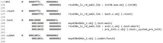
根据数据表、010h 是 P3REN 寄存器的存储器地址。

我尚未修改 CCS 生成的链接器脚本、并验证地址010h 是否已正确映射。

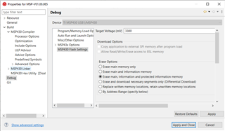
我还尝试选择了擦除主存储器、信息存储器和受保护的信息存储器区域的选项、但这并没有改变任何东西。

当我尝试闪存我从头开始编写的另一个(小)程序以测试器件(使一些 LED 闪烁等)时、闪存和调试工作无问题。

在刷写器件之前、我已将 具有 MSPFlasher 的器件存储器转储 到三个文件中:main.txt (main)、info.txt (info)、bootloader.txt (BSL):

C:\> MSP430Flasher -n MSP430FG4618 -r [main.txt,MAIN]
C:\> MSP430Flasher -n MSP430FG4618 -r [info.txt,INFO]
C:\> MSP430Flasher -n MSP430FG4618 -r [bootloader.txt,BSL]

当我尝试使用以下命令恢复旧固件时:

C:\> MSP430Flasher -n MSP430FG4618 -w main.txt -v -z [VCC=3300, RESET]
C:\> MSP430Flasher -n MSP430FG4618 -w info.txt -v -z [VCC=3300, RESET]
C:\> MSP430Flasher -n MSP430FG4618 -w bootloader.txt -v -z [VCC=3300, RESET]

main.txt 成功、但 info.txt 和 bootloader.txt 失败、并出现相同的错误:

* -----/|-------------------------------------------------------------------- *
*     / |__                                                                   *
*    /_   /   MSP Flasher v1.3.20                                             *
*      | /                                                                    *
* -----|/-------------------------------------------------------------------- *
*
* Evaluating triggers...done
* Checking for available FET debuggers:
* Found USB FET @ COM14 <- Selected
* Initializing interface @ COM14...done
* Checking firmware compatibility:
* FET firmware is up to date.
* Reading FW version...done
* Setting VCC to 3300 mV...done
* Accessing device...done
* Reading device information...done
* Loading file into device...
# Exit: 59
# ERROR: Could not write device memory
* Starting target code execution...done
* Disconnecting from device...done
*
* ----------------------------------------------------------------------------
* Driver      : closed (No error)
* ----------------------------------------------------------------------------
*/

这些问题的原因是什么? 如何进一步调查?

提前感谢您。

  • 请注意,本文内容源自机器翻译,可能存在语法或其它翻译错误,仅供参考。如需获取准确内容,请参阅链接中的英语原文或自行翻译。

    您好!

    以下主题类似、可帮助您解决问题。

    CCS/MSP430FG4618:文件加载器:在 slaa600d 中添加 BSL 时验证失败

  • 请注意,本文内容源自机器翻译,可能存在语法或其它翻译错误,仅供参考。如需获取准确内容,请参阅链接中的英语原文或自行翻译。

    您好!

    我查看 了您引用的论坛主题、并尝试了以下内容:

    1. 此处所述删除调试配置
    2. 删除工作区中的.metadata 文件夹并将工程重新导入 CCS。
    3. 创建新的工作区。
    4. 从工程文件夹中删除以下文件夹:
      • 启动
      • 设置
      • 调试
      • targetConfigs
    5. 删除上述文件夹、删除链接器脚本 lnk_MSP430FG4618.cmd、从工作区中删除项目并重新导入。
    6. 删除所有上述文件以及以下文件、然后创建新工作区并在现有源代码的文件夹中创建新项目:
      • ccsproject
      • .cproject
      • .project

    这一点都没有帮助。 我仍然收到相同的错误消息:

    MSP430: File Loader: Verification failed: Values at address 0x00010 do not match Please verify target memory and memory map.

    此外、我尝试对旧定制硬件的生产版本和 MSP-EXP430FG4618板进行编程、并且我在这两种情况下都遇到了相同的错误、这告诉我硬件不是问题、而是软件中的某个问题或如何构建硬件。

    错误消息显示我应该验证目标存储器和存储器映射。

    我能够在 Debug 文件夹中找到.map 文件。

    我看了一下它、我们的一个函数似乎位于名为 CODE_UPLD 的自定义代码段中、该代码段带有#pragma codeseg (我们之前的编译器)、我们已将 其更改为 TI-CGT 的#pragma CODE_SECTION。

    显然 、此段未在默认链接器脚本中映射、出于某种原因、链接器会将其映射到 映射文件中的地址00000010:

    SECTION ALLOCATION MAP
    
     output                                  attributes/
    section   page    origin      length       input sections
    --------  ----  ----------  ----------   ----------------
    CODE_UPLD 
    *          0    00000010    000000d0

    不过、我仍然对此感到困惑、因为8位外设寄存器的存储器映射应该对应于 RAM、但代码段应该存储在闪存中、所以 P3REN 应该映射到 RAM 地址0x10、而这个函数应该位于闪存的地址0x10、 这些地址空间应该是独立的、对吧?

    以下是 CCS 创建的链接器脚本的内容、我完全没有修改:

    /****************************************************************************/
    /* Specify the system memory map                                            */
    /****************************************************************************/
    
    MEMORY
    {
        SFR                     : origin = 0x0000, length = 0x0010
        PERIPHERALS_8BIT        : origin = 0x0010, length = 0x00F0
        PERIPHERALS_16BIT       : origin = 0x0100, length = 0x0100
        RAM                     : origin = 0x1100, length = 0x2000
        INFOA                   : origin = 0x1080, length = 0x0080
        INFOB                   : origin = 0x1000, length = 0x0080
        FLASH                   : origin = 0x3100, length = 0xCEBE
        FLASH2                  : origin = 0x10000,length = 0x10000
        BSLSIGNATURE            : origin = 0xFFBE, length = 0x0002, fill = 0xFFFF
        INT00                   : origin = 0xFFC0, length = 0x0002
        INT01                   : origin = 0xFFC2, length = 0x0002
        INT02                   : origin = 0xFFC4, length = 0x0002
        INT03                   : origin = 0xFFC6, length = 0x0002
        INT04                   : origin = 0xFFC8, length = 0x0002
        INT05                   : origin = 0xFFCA, length = 0x0002
        INT06                   : origin = 0xFFCC, length = 0x0002
        INT07                   : origin = 0xFFCE, length = 0x0002
        INT08                   : origin = 0xFFD0, length = 0x0002
        INT09                   : origin = 0xFFD2, length = 0x0002
        INT10                   : origin = 0xFFD4, length = 0x0002
        INT11                   : origin = 0xFFD6, length = 0x0002
        INT12                   : origin = 0xFFD8, length = 0x0002
        INT13                   : origin = 0xFFDA, length = 0x0002
        INT14                   : origin = 0xFFDC, length = 0x0002
        INT15                   : origin = 0xFFDE, length = 0x0002
        INT16                   : origin = 0xFFE0, length = 0x0002
        INT17                   : origin = 0xFFE2, length = 0x0002
        INT18                   : origin = 0xFFE4, length = 0x0002
        INT19                   : origin = 0xFFE6, length = 0x0002
        INT20                   : origin = 0xFFE8, length = 0x0002
        INT21                   : origin = 0xFFEA, length = 0x0002
        INT22                   : origin = 0xFFEC, length = 0x0002
        INT23                   : origin = 0xFFEE, length = 0x0002
        INT24                   : origin = 0xFFF0, length = 0x0002
        INT25                   : origin = 0xFFF2, length = 0x0002
        INT26                   : origin = 0xFFF4, length = 0x0002
        INT27                   : origin = 0xFFF6, length = 0x0002
        INT28                   : origin = 0xFFF8, length = 0x0002
        INT29                   : origin = 0xFFFA, length = 0x0002
        INT30                   : origin = 0xFFFC, length = 0x0002
        RESET                   : origin = 0xFFFE, length = 0x0002
    }
    
    /****************************************************************************/
    /* Specify the sections allocation into memory                              */
    /****************************************************************************/
    
    SECTIONS
    {
        .bss        : {} > RAM                  /* Global & static vars              */
        .data       : {} > RAM                  /* Global & static vars              */
        .TI.noinit  : {} > RAM                  /* For #pragma noinit                */
        .sysmem     : {} > RAM                  /* Dynamic memory allocation area    */
        .stack      : {} > RAM (HIGH)           /* Software system stack             */
    
    #ifndef __LARGE_CODE_MODEL__
        .text       : {} > FLASH                /* Code                              */
    #else
        .text       : {} >> FLASH2 | FLASH      /* Code                              */
    #endif
        .text:_isr  : {} > FLASH                /* ISR Code space                    */
        .cinit      : {} > FLASH                /* Initialization tables             */
    #ifndef __LARGE_DATA_MODEL__
        .const      : {} > FLASH                /* Constant data                     */
    #else
        .const      : {} >> FLASH | FLASH2      /* Constant data                     */
    #endif
        .bslsignature  : {} > BSLSIGNATURE      /* BSL Signature                     */
        .cio        : {} > RAM                  /* C I/O Buffer                      */
    
        .pinit      : {} > FLASH                /* C++ Constructor tables            */
        .binit      : {} > FLASH                /* Boot-time Initialization tables   */
        .init_array : {} > FLASH                /* C++ Constructor tables            */
        .mspabi.exidx : {} > FLASH              /* C++ Constructor tables            */
        .mspabi.extab : {} > FLASH              /* C++ Constructor tables            */
    #ifdef __TI_COMPILER_VERSION__
      #if __TI_COMPILER_VERSION__ >= 15009000
        #ifndef __LARGE_CODE_MODEL__
        .TI.ramfunc : {} load=FLASH, run=RAM, table(BINIT)
        #else
        .TI.ramfunc : {} load=FLASH | FLASH2, run=RAM, table(BINIT)
        #endif
      #endif
    #endif
    
        .infoA     : {} > INFOA              /* MSP430 INFO FLASH Memory segments */
        .infoB     : {} > INFOB
    
        /* MSP430 Interrupt vectors          */
        .int00       : {}               > INT00
        .int01       : {}               > INT01
        .int02       : {}               > INT02
        .int03       : {}               > INT03
        .int04       : {}               > INT04
        .int05       : {}               > INT05
        .int06       : {}               > INT06
        .int07       : {}               > INT07
        .int08       : {}               > INT08
        .int09       : {}               > INT09
        .int10       : {}               > INT10
        .int11       : {}               > INT11
        .int12       : {}               > INT12
        .int13       : {}               > INT13
        DAC12        : { * ( .int14 ) } > INT14 type = VECT_INIT
        DMA          : { * ( .int15 ) } > INT15 type = VECT_INIT
        BASICTIMER   : { * ( .int16 ) } > INT16 type = VECT_INIT
        PORT2        : { * ( .int17 ) } > INT17 type = VECT_INIT
        USART1TX     : { * ( .int18 ) } > INT18 type = VECT_INIT
        USART1RX     : { * ( .int19 ) } > INT19 type = VECT_INIT
        PORT1        : { * ( .int20 ) } > INT20 type = VECT_INIT
        TIMERA1      : { * ( .int21 ) } > INT21 type = VECT_INIT
        TIMERA0      : { * ( .int22 ) } > INT22 type = VECT_INIT
        ADC12        : { * ( .int23 ) } > INT23 type = VECT_INIT
        USCIAB0TX    : { * ( .int24 ) } > INT24 type = VECT_INIT
        USCIAB0RX    : { * ( .int25 ) } > INT25 type = VECT_INIT
        WDT          : { * ( .int26 ) } > INT26 type = VECT_INIT
        COMPARATORA   : { * ( .int27 ) } > INT27 type = VECT_INIT
        TIMERB1      : { * ( .int28 ) } > INT28 type = VECT_INIT
        TIMERB0      : { * ( .int29 ) } > INT29 type = VECT_INIT
        NMI          : { * ( .int30 ) } > INT30 type = VECT_INIT
        .reset       : {}               > RESET  /* MSP430 Reset vector         */
    }
    
    /****************************************************************************/
    /* Include peripherals memory map                                           */
    /****************************************************************************/
    
    -l msp430fg4618.cmd


    到目前为止、我还无法找到映射到闪存地址0x10的其他内容、从而导致与 CODE_UPLD 段冲突。

    如果我在链接器脚本中未指定、链接器会在哪里分配 CODE_UPLD 代码段?

    我在链接器脚本中看到以下行、但我不太理解其含义:

    #ifndef __LARGE_CODE_MODEL__
        .text       : {} > FLASH                /* Code                              */
    #else
        .text       : {} >> FLASH2 | FLASH      /* Code                              */
    #endif
        .text:_isr  : {} > FLASH                /* ISR Code space                    */

    在哪里可以找到有关链接器脚本语法的更多信息? 到目前为止、我只看到  了《MSP430优化 C/C++编译器 v21.6.0.LTS 用户指南》的第4.3.8节、该节非常简短、对该文件、尤其是代码段分配的精确语法解释不够。

    我找到了旧软件的段放置配置文件、该文件 将常规代码段映射到一个特定地址、将 CODE_UPLD 代码段映射到具有预定义大小的不同地址。

    如何将 CODE_UPLD 段映射到链接器脚本中的特定地址?

  • 请注意,本文内容源自机器翻译,可能存在语法或其它翻译错误,仅供参考。如需获取准确内容,请参阅链接中的英语原文或自行翻译。
    [引用 userid="459581" URL"~/support/microcontrollers/msp-low-power-microcontrollers-group/msp430/f/msp-low-power-microcontroller-forum/1019945/msp430fg4618-cannot-flash-device-with-ccs-or-mspflasher-verification-failed-values-at-address-0x00010-do-not-match/3769996 #3769996"]如果我没有在链接器脚本中指定 code_UPLD 代码段、链接器会在哪里分配该代码段?

    链接器将使用某些默认算法在存储器中创建和分配输出段"code_UPLD"、因为它未在链接器命令文件中显式分配。 一般而言、这是不可取的。 最好通过将段添加到链接器命令文件中的 SECTIONS 指令中、将段显式分配到适当的存储器区域。

    CCS 中的工程导入和编译错误(警告#10247-D:在不使用 SECTIONS 规范的情况下创建输出段"xxx")

    TI 链接器命令文件入门

    例如、假设您要在 FLASH2 |闪存范围内创建一个名为".code"的用户定义段、假设为大型代码模型。 使用默认链接器文件、我手动添加了".codeA"部分、如下所示。

    /****************************************************************************/
    /* Specify the sections allocation into memory                              */
    /****************************************************************************/
    
    SECTIONS
    {
        .bss        : {} > RAM                  /* Global & static vars              */
        .data       : {} > RAM                  /* Global & static vars              */
        .TI.noinit  : {} > RAM                  /* For #pragma noinit                */
        .sysmem     : {} > RAM                  /* Dynamic memory allocation area    */
        .stack      : {} > RAM (HIGH)           /* Software system stack             */
    
    #ifndef __LARGE_CODE_MODEL__
        .text       : {} > FLASH                /* Code                              */
    #else
        .text       : {} >> FLASH2 | FLASH      /* Code                              */
        .codeA      : {} >> FLASH2 | FLASH      /* Custom Code                       */
    #endif
        .text:_isr  : {} > FLASH                /* ISR Code space                    */
        .cinit      : {} > FLASH                /* Initialization tables             */
    #ifndef __LARGE_DATA_MODEL__
        .const      : {} > FLASH                /* Constant data                     */
    #else
        .const      : {} >> FLASH | FLASH2      /* Constant data                     */
    #endif
        .bslsignature  : {} > BSLSIGNATURE      /* BSL Signature                     */
        .cio        : {} > RAM                  /* C I/O Buffer                      */
    
        .pinit      : {} > FLASH                /* C++ Constructor tables            */
        .binit      : {} > FLASH                /* Boot-time Initialization tables   */
        .init_array : {} > FLASH                /* C++ Constructor tables            */
        .mspabi.exidx : {} > FLASH              /* C++ Constructor tables            */
        .mspabi.extab : {} > FLASH              /* C++ Constructor tables            */
    #ifdef __TI_COMPILER_VERSION__
      #if __TI_COMPILER_VERSION__ >= 15009000
        #ifndef __LARGE_CODE_MODEL__
        .TI.ramfunc : {} load=FLASH, run=RAM, table(BINIT)
        #else
        .TI.ramfunc : {} load=FLASH | FLASH2, run=RAM, table(BINIT)
        #endif
      #endif
    #endif
    
        .infoA     : {} > INFOA              /* MSP430 INFO FLASH Memory segments */
        .infoB     : {} > INFOB
    
        /* MSP430 Interrupt vectors          */
        .int00       : {}               > INT00
        .int01       : {}               > INT01
        .int02       : {}               > INT02
        .int03       : {}               > INT03
        .int04       : {}               > INT04
        .int05       : {}               > INT05
        .int06       : {}               > INT06
        .int07       : {}               > INT07
        .int08       : {}               > INT08
        .int09       : {}               > INT09
        .int10       : {}               > INT10
        .int11       : {}               > INT11
        .int12       : {}               > INT12
        .int13       : {}               > INT13
        DAC12        : { * ( .int14 ) } > INT14 type = VECT_INIT
        DMA          : { * ( .int15 ) } > INT15 type = VECT_INIT
        BASICTIMER   : { * ( .int16 ) } > INT16 type = VECT_INIT
        PORT2        : { * ( .int17 ) } > INT17 type = VECT_INIT
        USART1TX     : { * ( .int18 ) } > INT18 type = VECT_INIT
        USART1RX     : { * ( .int19 ) } > INT19 type = VECT_INIT
        PORT1        : { * ( .int20 ) } > INT20 type = VECT_INIT
        TIMERA1      : { * ( .int21 ) } > INT21 type = VECT_INIT
        TIMERA0      : { * ( .int22 ) } > INT22 type = VECT_INIT
        ADC12        : { * ( .int23 ) } > INT23 type = VECT_INIT
        USCIAB0TX    : { * ( .int24 ) } > INT24 type = VECT_INIT
        USCIAB0RX    : { * ( .int25 ) } > INT25 type = VECT_INIT
        WDT          : { * ( .int26 ) } > INT26 type = VECT_INIT
        COMPARATORA   : { * ( .int27 ) } > INT27 type = VECT_INIT
        TIMERB1      : { * ( .int28 ) } > INT28 type = VECT_INIT
        TIMERB0      : { * ( .int29 ) } > INT29 type = VECT_INIT
        NMI          : { * ( .int30 ) } > INT30 type = VECT_INIT
        .reset       : {}               > RESET  /* MSP430 Reset vector         */
    }

    然后、我修改了代码示例'msp430xG46x_1.c'并添加了一个名为"funcA"的函数、并使用"#pragma CODE_SECTION ()"将其放置在".codeA"段中。

    #include <msp430.h>
    
    #pragma CODE_SECTION(funcA,".codeA")
    int funcA(int a)
    {
     int i;
     return (i = a);
    }
    
    int main(void)

    映射文件显示此函数正被放置在主存储器的不同段中。

    [引用 userid="459581" URL"~/support/microcontrollers/msp-low-power-microcontrollers-group/msp430/f/msp-low-power-microcontroller-forum/1019945/msp430fg4618-cannot-flash-device-with-ccs-or-mspflasher-verification-failed-values-at-address-0x00010-do-not-match/3769996 #3769996"]如何将 CODE_UPLD 段映射到链接器脚本中的特定地址?

    我不想指定特定地址、而是使用上面所述的段将其放置在链接器选择的特定存储器范围中。 如果您不想将此自定义代码放置在闪存| FLASH2中、则可以在 链接器文件的存储器部分创建用户定义的段、该段使用某些主存储器。 这将要求您根据您放置段的位置来调整闪存或 FLASH2。

  • 请注意,本文内容源自机器翻译,可能存在语法或其它翻译错误,仅供参考。如需获取准确内容,请参阅链接中的英语原文或自行翻译。

    非常感谢。

    这解决了问题。

    我首先尝试了您建议的方法:

    [引用 userid="216616" URL"~/support/microcontrollers/msp-low-power-microcontrollers-group/msp430/f/msp-low-power-microcontroller-forum/1019945/msp430fg4618-cannot-flash-device-with-ccs-or-mspflasher-verification-failed-values-at-address-0x00010-do-not-match/3770828 #3770828"]我不会指定特定地址、而是使用上面所述的段将其放置在链接器选择的特定存储器范围内。

    这种情况非常好。

    但是、由于我可能必须重新生成上一个构建中的确切内存映射以实现向后兼容性、因此我还尝试在内存部分创建一个用户定义的段。

    为了完整起见、此处摘录了我在上下文中所做的更改:

    MEMORY
    {
        /* ... */
        FLASH                   : origin = 0x03100, length = 0x0CD00
        CODE_UPLD               : origin = 0x0FE00, length = 0x00120
        BSLSIGNATURE            : origin = 0x0FFBE, length = 0x00002, fill = 0xFFFF
        /* ... */
        FLASH2                  : origin = 0x10000, length = 0x10000
    }

    SECTIONS
    {
        /* ... */
        
    #ifndef __LARGE_CODE_MODEL__
        .text       : {} > FLASH                /* Code                              */
    #else
        .text       : {} >> FLASH2 | FLASH      /* Code                              */
    #endif
        CODE_UPLD   : {} > CODE_UPLD            /* Code                              */
        .text:_isr  : {} > FLASH                /* ISR Code space                    */
    
        /* ... */
    }

    这也没有问题。

  • 请注意,本文内容源自机器翻译,可能存在语法或其它翻译错误,仅供参考。如需获取准确内容,请参阅链接中的英语原文或自行翻译。
    [引用 userid="459581" URL"~/support/microcontrollers/msp-low-power-microcontrollers-group/msp430/f/msp-low-power-microcontroller-forum/1019945/msp430fg4618-cannot-flash-device-with-ccs-or-mspflasher-verification-failed-values-at-address-0x00010-do-not-match/3771724 #3771724"]

    非常感谢。

    这解决了问题。

    [/报价]

    很棒 感谢您发布您的方法并将问题标记为已解决!