This thread has been locked.

If you have a related question, please click the "Ask a related question" button in the top right corner. The newly created question will be automatically linked to this question.

[参考译文] MSP430FR4133:P1.7计时器 A0在具有精确设置的情况下工作、但无法正常工作 P8.3计时器 A1

Guru**** 657930 points
请注意,本文内容源自机器翻译,可能存在语法或其它翻译错误,仅供参考。如需获取准确内容,请参阅链接中的英语原文或自行翻译。

https://e2e.ti.com/support/microcontrollers/msp-low-power-microcontrollers-group/msp430/f/msp-low-power-microcontroller-forum/1214805/msp430fr4133-p1-7-timer-a0-works-but-not-p8-3-timer-a1-w-exact-settings

器件型号:MSP430FR4133

您好、我有一个非常简单的代码、该代码从 P8.1 A9上的电位器的 ADC 模块采样、以控制伺服电机 PWM、而后者又使 SG90伺服电机旋转。

以下代码适用于 PWM 信号的 P1.7输出并使用计时器 TA0模块

// Main c file 

/********************************
main.c
Default Template file for testing purposes
Aaron Shek, @ 2023 University of Strathclyde
*********************************/

#include <msp430.h>
#include <driverlib.h>
#include <stdio.h>

unsigned int rate_ = 0;
uint32_t TimerA0_period = 20000; // PWM Period
unsigned int i;

// ADC interrupt service routine
#pragma vector=ADC_VECTOR           
__interrupt void ADC_ISR(void)
{
  switch(__even_in_range(ADCIV,ADCIV_ADCIFG))
  {
    case ADCIV_ADCIFG:              
    rate_ = (int)(600 + (2.05*ADCMEM0)); // Max value of 2695, min 600
    //printf("%d\n",rate_);
    __bic_SR_register_on_exit(LPM0_bits); // Clear CPUOFF bit from LMP0 to prevent MCU sleeping
    //ADC_clearInterrupt(ADC_BASE,ADC_COMPLETED_INTERRUPT);
    break;
  }
}

void main(void)
{
    WDTCTL = WDTPW | WDTHOLD; // Stop WDT
    
    P1DIR |= 0x80; // P1.7 output
    P1SEL0 |= 0x80; // P1.7 options select
    
    P4DIR |= 0x01; // Indicator LED
    P4OUT |= 0x01; 
    
    // Configure Pin for ADC
    GPIO_setAsPeripheralModuleFunctionOutputPin(GPIO_PORT_P8,GPIO_PIN1,GPIO_PRIMARY_MODULE_FUNCTION);
    
    // Disable the GPIO power-on default high-impedance mode to activate
    // previously configured port settings
    PM5CTL0 &= ~LOCKLPM5; PMM_unlockLPM5();
    
    // Timer TA0 setup
    TA0CCR0 = TimerA0_period; // PWM Period
    TA0CCTL1 = OUTMOD_7; // CCR1 reset/set                      
    TA0CTL = TASSEL_2 | MC_1; // SMCLK, up mode
    
    // ADC setup
    // Configure the Pin
    SYSCFG2 |= ADCPCTL9; // Turn on analogue pin A9 (so it is not a GPIO).
    // Configure CLock source, operation mode
    ADCCTL0 |= ADCSHT_2 | ADCON;  // 16 ADCCLK cycles, turn on ADC.
    ADCCTL1 |= ADCSHP; // ADDCLK = MODOSC; sampling timer
    ADCCTL2 |= ADCRES; // 10 bit conversion results
    // Configure ADC mux and +ve & -ve references
    ADCMCTL0 |= ADCINCH_9; // A9 ADC input select; Vref = AVCC   
    ADCIFG &= ~0x01;  //Clear interrupt flag  
    ADCIE |= ADCIE0;  //Enable ADC conversion complete interrupt
 
    __enable_interrupt();
      
    while(1) {  
      ADCCTL0 |= 0x03;          // Sampling and conversion start
      while(ADCCTL0 & ADCBUSY) {
      int memval = rate_;
      TA0CCR1 = memval;     
      __delay_cycles(10000);
      }
    }  
    // __bis_SR_register(LPM0_bits); // Enter LPM0
    
}

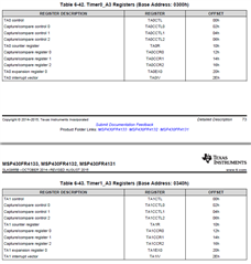
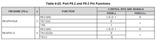
然而、当我想改用 P8.3与 计时器 TA1模块一起使用、而改用完全相同的配置时、不起作用:  

// Main c file 

/********************************
main.c
Default Template file for testing purposes
Aaron Shek, @ 2023 University of Strathclyde
*********************************/

#include <msp430.h>
#include <driverlib.h>
#include <stdio.h>

unsigned int rate_ = 0;
uint32_t TimerA1_period = 20000; // PWM Period
unsigned int i;

// ADC interrupt service routine
#pragma vector=ADC_VECTOR           
__interrupt void ADC_ISR(void)
{
  switch(__even_in_range(ADCIV,ADCIV_ADCIFG))
  {
    case ADCIV_ADCIFG:              
    rate_ = (int)(600 + (2.05*ADCMEM0)); // Max value of 2695, min 600
    //printf("%d\n",rate_);
    __bic_SR_register_on_exit(LPM0_bits); // Clear CPUOFF bit from LMP0 to prevent MCU sleeping
    //ADC_clearInterrupt(ADC_BASE,ADC_COMPLETED_INTERRUPT);
    break;
  }
}

void main(void)
{
    WDTCTL = WDTPW | WDTHOLD; // Stop WDT
    
    P8DIR |= 0x03; // P8.3 output
    P8SEL0 |= 0x03; // P8.3 options select
    
    P4DIR |= 0x01; // Indicator LED
    P4OUT |= 0x01; 
    
    // Configure Pin for ADC
    GPIO_setAsPeripheralModuleFunctionOutputPin(GPIO_PORT_P8,GPIO_PIN1,GPIO_PRIMARY_MODULE_FUNCTION);
    
    // Disable the GPIO power-on default high-impedance mode to activate
    // previously configured port settings
    PM5CTL0 &= ~LOCKLPM5; PMM_unlockLPM5();
    
    // Timer TA0 setup
    TA1CCR0 = TimerA1_period; // PWM Period
    TA1CCTL1 = OUTMOD_7; // CCR1 reset/set                      
    TA1CTL = TASSEL_2 | MC_1; // SMCLK, up mode
    
    // ADC setup
    // Configure the Pin
    SYSCFG2 |= ADCPCTL9; // Turn on analogue pin A9 (so it is not a GPIO).
    // Configure CLock source, operation mode
    ADCCTL0 |= ADCSHT_2 | ADCON;  // 16 ADCCLK cycles, turn on ADC.
    ADCCTL1 |= ADCSHP; // ADDCLK = MODOSC; sampling timer
    ADCCTL2 |= ADCRES; // 10 bit conversion results
    // Configure ADC mux and +ve & -ve references
    ADCMCTL0 |= ADCINCH_9; // A9 ADC input select; Vref = AVCC   
    ADCIFG &= ~0x01;  //Clear interrupt flag  
    ADCIE |= ADCIE0;  //Enable ADC conversion complete interrupt
 
    __enable_interrupt();
      
    while(1) {  
      ADCCTL0 |= 0x03;          // Sampling and conversion start
      while(ADCCTL0 & ADCBUSY) {
      int memval = rate_;
      TA1CCR1 = memval;     
      __delay_cycles(10000);
      }
    }  
    // __bis_SR_register(LPM0_bits); // Enter LPM0
}

我迷路了、而且我查阅了用户指南和数据表、但我看不出哪里出错了。  

非常感谢您的帮助。

亚伦

  • 请注意,本文内容源自机器翻译,可能存在语法或其它翻译错误,仅供参考。如需获取准确内容,请参阅链接中的英语原文或自行翻译。

        P8DIR |= 0x03; // P8.3 output
        P8SEL0 |= 0x03; // P8.3 options select
     

    这些位适用于 P8.0和 P8.1。 您需要的是器件头文件中提供的方便符号 BIT3 (0x08)。

  • 请注意,本文内容源自机器翻译,可能存在语法或其它翻译错误,仅供参考。如需获取准确内容,请参阅链接中的英语原文或自行翻译。

    尊敬的 David:

    感谢您的答复。 很遗憾、当我从0x03更改为 BIT3时、它似乎没有修复。  

  • 请注意,本文内容源自机器翻译,可能存在语法或其它翻译错误,仅供参考。如需获取准确内容,请参阅链接中的英语原文或自行翻译。

    这很简单、就像您从使用 CCR1更改到使用 CCR2一样? 您使用的第一个迭代 P1.7/ TA0.1 即计时器 A0、CCR1。 您更改为 P8.3/ TA1.2  即计时器 A1、CCR2。  在您的代码中、您正确地从 TA0更改为 TA1、但从 CCTL1更改为 CCTL2或从 CCR1更改为 CCR2。

    编辑:您仍需要包括 David 提到的更改。

  • 请注意,本文内容源自机器翻译,可能存在语法或其它翻译错误,仅供参考。如需获取准确内容,请参阅链接中的英语原文或自行翻译。

    谢谢你的回应,这似乎是有希望的第一,但仍然没有运气,我已经附上了代码。

    // Main c file 
    
    /********************************
    main.c
    Default Template file for testing purposes
    Aaron Shek, @ 2023 University of Strathclyde
    *********************************/
    
    #include <msp430.h>
    #include <driverlib.h>
    #include <stdio.h>
    
    unsigned int rate_ = 0;
    uint32_t TimerA1_period = 20000; // PWM Period
    unsigned int i;
    
    // ADC interrupt service routine
    #pragma vector=ADC_VECTOR           
    __interrupt void ADC_ISR(void)
    {
      switch(__even_in_range(ADCIV,ADCIV_ADCIFG))
      {
        case ADCIV_ADCIFG:              
        rate_ = (int)(600 + (2.05*ADCMEM0)); // Max value of 2695, min 600
        //printf("%d\n",rate_);
        __bic_SR_register_on_exit(LPM0_bits); // Clear CPUOFF bit from LMP0 to prevent MCU sleeping
        //ADC_clearInterrupt(ADC_BASE,ADC_COMPLETED_INTERRUPT);
        break;
      }
    }
    
    void main(void)
    {
        WDTCTL = WDTPW | WDTHOLD; // Stop WDT
        
        P8DIR |= BIT3; // P8.3 output
        P8SEL0 |= BIT3; // P8.3 options select
        
        P4DIR |= 0x01; // Indicator LED
        P4OUT |= 0x01; 
        
        // Configure Pin for ADC
        GPIO_setAsPeripheralModuleFunctionOutputPin(GPIO_PORT_P8,GPIO_PIN1,GPIO_PRIMARY_MODULE_FUNCTION);
        
        // Disable the GPIO power-on default high-impedance mode to activate
        // previously configured port settings
        PM5CTL0 &= ~LOCKLPM5; PMM_unlockLPM5();
        
        // Timer TA1 setup
        TA1CCR1 = TimerA1_period; // PWM Period
        TA1CCTL2 = OUTMOD_7; // CCR1 reset/set                      
        TA1CTL = TASSEL_2 | MC_1; // SMCLK, up mode
        
        // ADC setup
        // Configure the Pin
        SYSCFG2 |= ADCPCTL9; // Turn on analogue pin A9 (so it is not a GPIO).
        // Configure CLock source, operation mode
        ADCCTL0 |= ADCSHT_2 | ADCON;  // 16 ADCCLK cycles, turn on ADC.
        ADCCTL1 |= ADCSHP; // ADDCLK = MODOSC; sampling timer
        ADCCTL2 |= ADCRES; // 10 bit conversion results
        // Configure ADC mux and +ve & -ve references
        ADCMCTL0 |= ADCINCH_9; // A9 ADC input select; Vref = AVCC   
        ADCIFG &= ~0x01;  //Clear interrupt flag  
        ADCIE |= ADCIE0;  //Enable ADC conversion complete interrupt
     
        __enable_interrupt();
          
        while(1) {  
          ADCCTL0 |= 0x03;          // Sampling and conversion start
          while(ADCCTL0 & ADCBUSY) {
          int memval = rate_;
          TA1CCR2 = memval;     
          __delay_cycles(10000);
          }
        }  
        // __bis_SR_register(LPM0_bits); // Enter LPM0
    }

    如果您查看寄存器、timer0和 Timer1是相同的、那么从逻辑上讲应该相同的。  

    非常感谢。  

    亚伦

  • 请注意,本文内容源自机器翻译,可能存在语法或其它翻译错误,仅供参考。如需获取准确内容,请参阅链接中的英语原文或自行翻译。

    Aaron、

    调试项目、并在处于 while 环路中时检查端口8的 GPIO 设置。 您用来设置 ADC 的 driverlib 函数很可能会覆盖您在上面为设置计时器输出所做的事情、因为它们是同一个端口。  

    此外、由于计时器不是32位、因此 PWM 周期应更改为 uint16_t 变量。 这将更改 底层容器大小并减少 CPU 开销。  

  • 请注意,本文内容源自机器翻译,可能存在语法或其它翻译错误,仅供参考。如需获取准确内容,请参阅链接中的英语原文或自行翻译。

    为了补充 Jace 的注释、修订后的代码未 设置 CCR0寄存器的值。 在最新代码片段的第50行、您要为 CCR1设置 TimerA1_PERIOD、而不是所需的 CCR0。 请牢记、在用户指南中、"定时器重复计数增加至比较寄存器 TAxCCR0的值、这个值定义了周期"。

  • 请注意,本文内容源自机器翻译,可能存在语法或其它翻译错误,仅供参考。如需获取准确内容,请参阅链接中的英语原文或自行翻译。

    谢谢、这解决了我的问题。 还感谢 Jace 关于变量类型的建议。