This thread has been locked.

If you have a related question, please click the "Ask a related question" button in the top right corner. The newly created question will be automatically linked to this question.

TMS320F28027: 通过UniFlash或C2Prog烧录加密过的程序,程序不运行

Part Number: TMS320F28027
Other Parts Discussed in Thread: UNIFLASH, C2000WARE, MOTORWARE

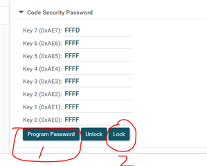
问题:用CCS11.1.0通过添加 CSMPasswords.asm文件的方式对程序进行加密,

1.加密后的程序,用CCS第一次烧录,一切正常,可以正常运行。然后第二次再烧同样的加密程序,烧录不进。报错

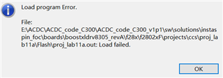
2.用UniFlash或C2Prog烧录未加密的程序,一切正常。烧录加密后的.out文件,烧录过程没有报错,但程序不运行。

请问是怎么回事?

我希望能够用UniFlash或C2Prog烧录加密后的程序并正常运行,而且能够反复烧录未改密码的程序,CCS也是一样能够反复烧录未改密码的程序,希望能帮我解决,谢谢

  • 1、第一次烧写成功后芯片就处于加密状态,此时如果要再次烧写,那要先对芯片解密后才能连接和烧写。

    2、这个要看你烧写的程序是烧写到ram了还是flash了?可以根据你的cmd文件判断,cmd文件中带ram字样,那程序是烧写到ram,掉电后就丢失了。反之flash字样的是可以离线运行的。

    建议你可以使用例程测试导致的无法烧写/运行,一方面GPIO的运行也方便测试:C:\ti\c2000\C2000Ware_4_01_00_00\device_support\f2802x\examples\drivers\gpio_toggle

    烧写之前编译的时候,点击编译摁扭旁边的倒三角,选择“flash”编译,烧写的时候就会烧写进flash。

  • 我的CMD文件是F28027F.cmd应该是烧写进flash了,因为不带密码的程序,烧写进去,掉电是能运行的

  • 你好,现在是不加密的程序烧写进芯片可以运行了?只有加密之后的程序无法运行?

    是同一个程序吗,如果是同一个程序那如果正确加密的话是不影响运行的。如果不是同一个的话可能跟程序里的某些设置有关,比如有些程序(delay_us函数)的使用需要调用memcpy函数。

  • 是同一个程序,是通过添加CSMPasswords.asm文件的方式对程序进行加密的,enableCSM .set 0 ;0-disable CSM, 1-enable CSM

    使能加密,用UniFlash或C2Prog烧录进去不能运行,但用CCS烧录能运行。禁能加密,用UniFlash或C2Prog烧录进去就能运行

  • 确实没测试过用Uniflash或C2Prog烧写加密的程序,但是至少用CCS生成的.out在CCS中和在unilfash中烧写应该是效果一样的。

    如果用uniflash烧写未加密工程,然后再在uniflash的OTP中修改密码进行加密后程序是否能正常运行?

  • 你是说通过点击uniflash中的这两个按键进行加密吗,我试了,先下载没加密的程序,然后点击这两个按键进行加密。也是不能运行。

  • /*
    // TI File $Revision: /main/7 $
    // Checkin $Date: July 6, 2009   17:25:36 $
    //###########################################################################
    //
    // FILE:  F28027.cmd
    //
    // TITLE: Linker Command File For F28027 Device
    //
    //###########################################################################
    // $TI Release: 2802x C/C++ Header Files and Peripheral Examples V1.29 $
    // $Release Date: January 11, 2011 $
    //###########################################################################
    */
    
    /* ======================================================
    // For Code Composer Studio V2.2 and later
    // ---------------------------------------
    // In addition to this memory linker command file,
    // add the header linker command file directly to the project.
    // The header linker command file is required to link the
    // peripheral structures to the proper locations within
    // the memory map.
    //
    // The header linker files are found in <base>\DSP2802_Headers\cmd
    //
    // For BIOS applications add:      DSP2802x_Headers_BIOS.cmd
    // For nonBIOS applications add:   DSP2802x_Headers_nonBIOS.cmd
    ========================================================= */
    
    /* ======================================================
    // For Code Composer Studio prior to V2.2
    // --------------------------------------
    // 1) Use one of the following -l statements to include the
    // header linker command file in the project. The header linker
    // file is required to link the peripheral structures to the proper
    // locations within the memory map                                    */
    
    /* Uncomment this line to include file only for non-BIOS applications */
    /* -l DSP2802x_Headers_nonBIOS.cmd */
    
    /* Uncomment this line to include file only for BIOS applications */
    /* -l DSP2802x_Headers_BIOS.cmd */
    
    /* 2) In your project add the path to <base>\DSP2802x_headers\cmd to the
       library search path under project->build options, linker tab,
       library search path (-i). */
    /*========================================================= */
    
    /* Define the memory block start/length for the F28027
       PAGE 0 will be used to organize program sections
       PAGE 1 will be used to organize data sections
    
       Notes:
             Memory blocks on F2802x are uniform (ie same
             physical memory) in both PAGE 0 and PAGE 1.
             That is the same memory region should not be
             defined for both PAGE 0 and PAGE 1.
             Doing so will result in corruption of program
             and/or data.
    
             The L0 memory block is mirrored - that is
             it can be accessed in high memory or low memory.
             For simplicity only one instance is used in this
             linker file.
    
             Contiguous SARAM memory blocks or flash sectors can be
             be combined if required to create a larger memory block.
    */
    
    MEMORY
    {
    PAGE 0:    /* Program Memory */
               /* Memory (RAM/FLASH/OTP) blocks can be moved to PAGE1 for data allocation */
    
       OTP         : origin = 0x3D7800, length = 0x000400     /* on-chip OTP */
       CSM_RSVD    : origin = 0x3F7F80, length = 0x000076     /* Part of FLASHA.  Program with all 0x0000 when CSM is in use. */
       BEGIN       : origin = 0x3F7FF6, length = 0x000002     /* Part of FLASHA.  Used for "boot to Flash" bootloader mode. */
       CSM_PWL_P0  : origin = 0x3F7FF8, length = 0x000008     /* Part of FLASHA.  CSM password locations in FLASHA */
    
       IQTABLES    : origin = 0x3FE000, length = 0x000B50     /* IQ Math Tables in Boot ROM */
       IQTABLES2   : origin = 0x3FEB50, length = 0x00008C     /* IQ Math Tables in Boot ROM */
       IQTABLES3   : origin = 0x3FEBDC, length = 0x0000AA     /* IQ Math Tables in Boot ROM */
    
       ROM         : origin = 0x3FF27C, length = 0x000D44     /* Boot ROM */
       RESET       : origin = 0x3FFFC0, length = 0x000002     /* part of boot ROM  */
       VECTORS     : origin = 0x3FFFC2, length = 0x00003E     /* part of boot ROM  */
       FLASHB_D    : origin = 0x3F0000, length = 0x006000     /* on-chip FLASH B, C and D */
       D_FLASHA    : origin = 0x3F6000, length = 0x001F80     /* on-chip FLASH A */
       P_RAML0     : origin = 0x008000, length = 0x000980     /* on-chip PRAM block L0 */
    
    PAGE 1 :   /* Data Memory */
               /* Memory (RAM/FLASH/OTP) blocks can be moved to PAGE0 for program allocation */
               /* Registers remain on PAGE1                                                  */
    
       RAMM0_M1    : origin = 0x000000, length = 0x000600     /* on-chip RAM block M0 + M1. 0x600 to 0x800 reserved for InstaSPIN */
       D_RAML0     : origin = 0x008980, length = 0x000680     /* on-chip DRAM block L0 */
    }
    
    /* Allocate sections to memory blocks.
       Note:
             codestart user defined section in DSP28_CodeStartBranch.asm used to redirect code
                       execution when booting to flash
             ramfuncs  user defined section to store functions that will be copied from Flash into RAM
    */
    
    SECTIONS
    {
       /* Allocate program areas: */
       .cinit              : > FLASHB_D     PAGE = 0
       .pinit              : > FLASHB_D,    PAGE = 0
       .text               : > FLASHB_D     PAGE = 0
       codestart           : > BEGIN        PAGE = 0
       ramfuncs            : LOAD = FLASHB_D,
                             RUN = P_RAML0,
                             LOAD_START(_RamfuncsLoadStart),
                             LOAD_END(_RamfuncsLoadEnd),
                             RUN_START(_RamfuncsRunStart),
                             PAGE = 0
    
       csmpasswds          : > CSM_PWL_P0   PAGE = 0
       csm_rsvd            : > CSM_RSVD     PAGE = 0
    
       /* Allocate uninitalized data sections: */
       .stack              : > D_RAML0     PAGE = 1
       .ebss               : > RAMM0_M1     PAGE = 1
       .esysmem            : > RAMM0_M1     PAGE = 1
    
       ebss_extension      : > P_RAML0      PAGE = 0
       rom_accessed_data   : > RAMM0_M1     PAGE = 1
    
       vib_buf_data	       : > D_RAML0      PAGE = 1
       graph_data		   : > D_RAML0      PAGE = 1
    
       /* Initalized sections go in Flash */
       /* For SDFlash to program these, they must be allocated to page 0 */
       .econst             : > D_FLASHA,    PAGE = 0
       .switch             : > D_FLASHA,    PAGE = 0
    
       /* Allocate IQ math areas: */
       IQmath              : > FLASHB_D     PAGE = 0            /* Math Code */
       IQmathTables        : > IQTABLES,    PAGE = 0, TYPE = NOLOAD
    
       /* Uncomment the section below if calling the IQNexp() or IQexp()
          functions from the IQMath.lib library in order to utilize the
          relevant IQ Math table in Boot ROM (This saves space and Boot ROM
          is 1 wait-state). If this section is not uncommented, IQmathTables2
          will be loaded into other memory (SARAM, Flash, etc.) and will take
          up space, but 0 wait-state is possible.
       */
       /*
       IQmathTables2    : > IQTABLES2, PAGE = 0, TYPE = NOLOAD
       {
    
                  IQmath.lib<IQNexpTable.obj> (IQmathTablesRam)
    
       }
       */
       /* Uncomment the section below if calling the IQNasin() or IQasin()
          functions from the IQMath.lib library in order to utilize the
          relevant IQ Math table in Boot ROM (This saves space and Boot ROM
          is 1 wait-state). If this section is not uncommented, IQmathTables3
          will be loaded into other memory (SARAM, Flash, etc.) and will take
          up space, but 0 wait-state is possible.
       */
       /*
       IQmathTables3    : > IQTABLES3, PAGE = 0, TYPE = NOLOAD
       {
    
                  IQmath.lib<IQNasinTable.obj> (IQmathTablesRam)
    
       }
       */
    
       /* .reset is a standard section used by the compiler.  It contains the */
       /* the address of the start of _c_int00 for C Code.  */
       /* When using the boot ROM this section and the CPU vector */
       /* table is not needed.  Thus the default type is set here to  */
       /* DSECT  */
       .reset              : > RESET,      PAGE = 0, TYPE = DSECT
       vectors             : > VECTORS     PAGE = 0, TYPE = DSECT
    
    }
    
    /*
    //===========================================================================
    // End of file.
    //===========================================================================
    */

    这个问题不知道和CMD文件有关系没,我的工程是基于C:\ti\motorware\motorware_1_01_00_18\sw\solutions\instaspin_foc\boards\boostxldrv8305_revA\f28x\f2802xF\projects\ccs\proj_lab11a建立的,CMD文件是F28027F.cmd。上面是cmd中的内容

  • 我也有考虑cmd文件的问题,但是你说到工程使用CCS烧写是可以正确加密和运行的,所以就把这个问题否了。

    你可以再试试使用lab11a的原始cmd文件,然后在cmd文件中修改csm相关的语句,在cmd中加入这些语句:

    MEMORY
     {
    
    …
    CSM_RSVD : origin = 0x3F7F80, length = 0x000076
    …
    CSM_PWL : origin = 0x3F7FF8, length = 0x000008
    …
    }
    SECTIONS
     {
    …
    csmpasswds : > CSM_PWL PAGE = 0
    
    …
    csm_rsvd : > CSM_RSVD PAGE = 0
    …
    }

    另外,

    你是说通过点击uniflash中的这两个按键进行加密吗,我试了,先下载没加密的程序,然后点击这两个按键进行加密。也是不能运行。

    进行这些操作的时候有没有将工程恢复到没有添加csm的情况?

  • 这恐怕要麻烦你前往英文E2E论坛咨询一下这个情况了:e2e.ti.com/.../c2000-microcontrollers-forum