This thread has been locked.

If you have a related question, please click the "Ask a related question" button in the top right corner. The newly created question will be automatically linked to this question.

TMS320F280025: 关于模拟子系统中的ADCDACLOOPBACK寄存器

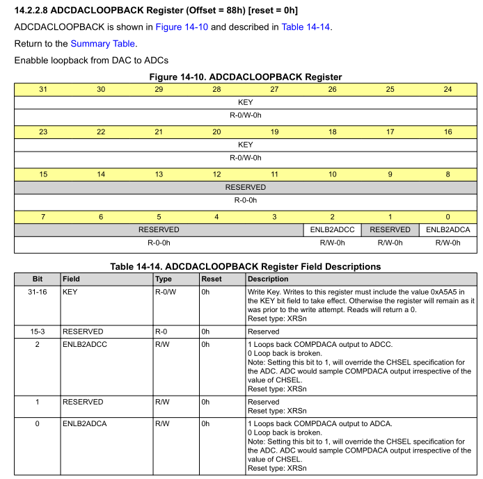
Part Number: TMS320F280025


如下图,没有在TRM、DS文件中找到关于LoopBack DAC到ADC的框图,请问:

(1)哪里有结构框图?想看看如何loopback的。

(2)模拟子系统包括4个比较器,每个比较器包括高端和低端共2个DAC,那4个比较器就是有8个DAC了。下面的寄存器的字段ENLB2ADCA,ENLB2ADCC描述不够清晰,

COMPDACA指的是哪个DAC,以及连接到了ADCA和ADCC的哪些通道?还是说的框图的问题。

谢谢!

  • 你好,确实描述不够清晰,我将咨询相关资深工程师,一旦有回复会立即回复您。

  • 你好,请查看以下工程师的回复:

    When the loopback bit is set, the ADC will sample the output of CMPSS1 DACL (low DAC). As long as the bit is set, the configured ADC will sample the DACL output regardless of what channel is selected (the loopback setting overrides CHSEL). There is a special acquisition window requirement when sampling the internal COMPDAC output - at least 4.3us (430 cycles at 100MHz SYSCLK). The DAC output effectively has a 7-bit resolution in this case, even though the input to DACLVALA is a 12-bit value (IOW, discard the last 5 LSBs).

    This feature is intended for use as a diagnostic/self-test mechanism to confirm that ADCs are converting properly.