

在下载完CPU1后会接着自动把CPU1的程序下载到CPU2里面去。记得第一次下载的时候有弹出一个框让我选择下载到哪个核,现在不知道这个框在哪里打开。
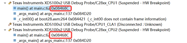
现在想CPU1的程序烧录到CPU1核,CPU2的程序烧录到CPU2该怎么操作?
C28xx_CPU1: GEL Output:
Memory Map Initialization Complete
C28xx_CPU1: GEL Output:
... DCSM Initialization Start ...
C28xx_CPU1: GEL Output:
... DCSM Initialization Done ...
C28xx_CPU1: GEL Output:
CPU2 is out of reset and configured to wait boot.
(If you connected previously, may have to resume CPU2 to reach wait boot loop.)
C28xx_CPU1: GEL Output:
CM is out of reset and configured to wait boot.
(If you connected previously, may have to resume CM to reach wait boot loop.)
C28xx_CPU1: If erase/program (E/P) operation is being done on one core, the other core should not execute from shared-RAM (SR) as they are used for the E/P code. User code execution from SR could commence after both flash banks are programmed.
C28xx_CPU1: Only CPU1 on-chip Flash Plugin can configure clock for CPU1, CPU2 and CM Flash operations. Plugin automatically configures PLL when CPU1 Flash operations are invoked. However, if users want to do only CPU2 or CM Flash operations without doing a prior CPU1 operation in the current session, they should click on 'Configure Clock' button in CPU1's on-chip Flash Plugin before invoking CPU2 and CM Flash operations. When this button is used, Flash Plugin will configure the clock for CPU1/CPU2 at 190MHz and CM at 95MHz using INTOSC2 as the clock source. Plugin will leave PLL config like this and user application should configure the PLL as required by application.
C28xx_CPU1: GEL Output:
... DCSM Initialization Start ...
C28xx_CPU1: GEL Output:
... DCSM Initialization Done ...
C28xx_CPU1: GEL Output:
CPU2 is out of reset and configured to wait boot.
(If you connected previously, may have to resume CPU2 to reach wait boot loop.)
C28xx_CPU1: GEL Output:
CM is out of reset and configured to wait boot.
(If you connected previously, may have to resume CM to reach wait boot loop.)
C28xx_CPU1: Loader: One or more sections of your program falls into a memory region that is not writable. These regions will not actually be written to the target. Check your linker configuration and/or memory map.
C28xx_CPU1: GEL Output:
... DCSM Initialization Start ...
C28xx_CPU1: GEL Output:
... DCSM Initialization Done ...
C28xx_CPU1: GEL Output:
CPU2 is out of reset and configured to wait boot.
(If you connected previously, may have to resume CPU2 to reach wait boot loop.)
C28xx_CPU1: GEL Output:
CM is out of reset and configured to wait boot.
(If you connected previously, may have to resume CM to reach wait boot loop.)
C28xx_CPU2: GEL Output:
Memory Map Initialization Complete
C28xx_CPU2: If erase/program (E/P) operation is being done on one core, the other core should not execute from shared-RAM (SR) as they are used for the E/P code. User code execution from SR could commence after both flash banks are programmed.
C28xx_CPU2: Only CPU1 on-chip Flash Plugin can configure clock for CPU1, CPU2 and CM Flash operations. Plugin automatically configures PLL when CPU1 Flash operations are invoked. However, if users want to do only CPU2 or CM Flash operations without doing a prior CPU1 operation in the current session, they should click on 'Configure Clock' button in CPU1's on-chip Flash Plugin before invoking CPU2 and CM Flash operations. When this button is used, Flash Plugin will configure the clock for CPU1/CPU2 at 190MHz and CM at 95MHz using INTOSC2 as the clock source. Plugin will leave PLL config like this and user application should configure the PLL as required by application.
C28xx_CPU2: Loader: One or more sections of your program falls into a memory region that is not writable. These regions will not actually be written to the target. Check your linker configuration and/or memory map.

