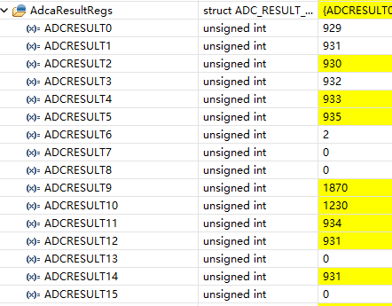
程序中ADC转换结果只有实际值的一半,比如1.52V的输入电压,ADC结果为930,而实际ADC结果应该为 (1.52/3.3)*4096=1886
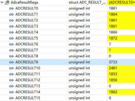
检查自己的工程,没有发现配置问题,然后用Ti的例程adc_ex1_soc_epwm来测试,结果仍然如此。
ADC采用内部参考电压3.3V
TI例程中的部分代码:
void initADC(void)
{
//
// Setup VREF as internal
//
SetVREF(ADC_ADCA, ADC_INTERNAL, ADC_VREF3P3);
EALLOW;
//
// Set ADCCLK divider to /4
//
AdcaRegs.ADCCTL2.bit.PRESCALE = 6;
//
// Set pulse positions to late
//
AdcaRegs.ADCCTL1.bit.INTPULSEPOS = 1;
//
// Power up the ADC and then delay for 1 ms
//
AdcaRegs.ADCCTL1.bit.ADCPWDNZ = 1;
EDIS;
DELAY_US(1000);
}
void SetVREF(int module, int mode, int ref)
{
Uint16 *offset, offsetShiftVal;
if((mode == ADC_INTERNAL) && (ref == ADC_VREF3P3))
{
offsetShiftVal = 8U; // Internal / 1.65v mode offset
}
else
{
offsetShiftVal = 0U; // All other modes
}
//
// Set up pointer to offset trim in OTP for ADCA.
//
offset = (Uint16 *)((Uint32)0x7016CU);
EALLOW;
//
// Get offset trim from OTP and write it to the register for ADCA.
//
AdcaRegs.ADCOFFTRIM.bit.OFFTRIM = (*offset >> offsetShiftVal) & 0xFFU;
//
// Set up pointer to offset trim in OTP for ADCB.
//
offset = (Uint16 *)((Uint32)0x7016DU);
//
// Get offset trim from OTP and write it to the register for ADCB.
//
AdcbRegs.ADCOFFTRIM.bit.OFFTRIM = (*offset >> offsetShiftVal) & 0xFFU;
//
// Set up pointer to offset trim in OTP for ADCC.
//
offset = (Uint16 *)((Uint32)0x7016EU);
//
// Get offset trim from OTP and write it to the register for ADCC.
//
AdccRegs.ADCOFFTRIM.bit.OFFTRIM = (*offset >> offsetShiftVal) & 0xFFU;
//
// Configure the reference mode for all ADCs (internal or external).
//
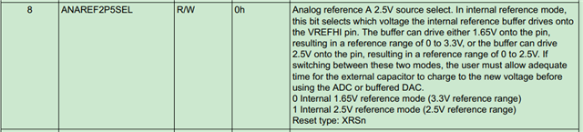
AnalogSubsysRegs.ANAREFCTL.bit.ANAREFSEL = mode;
//
// Configure the reference voltage for all ADCs (3.3V or 2.5V).
//
AnalogSubsysRegs.ANAREFCTL.bit.ANAREF2P5SEL = ref;
EDIS;
}
void initADCSOC(void)
{
//
// Select the channels to convert and the end of conversion flag
//
EALLOW;
AdcaRegs.ADCSOC0CTL.bit.CHSEL = 1; // SOC0 will convert pin A1
// 0:A0 1:A1 2:A2 3:A3
// 4:A4 5:A5 6:A6 7:A7
// 8:A8 9:A9 A:A10 B:A11
// C:A12 D:A13 E:A14 F:A15
AdcaRegs.ADCSOC0CTL.bit.ACQPS = 9; // Sample window is 10 SYSCLK cycles
AdcaRegs.ADCSOC0CTL.bit.TRIGSEL = 5; // Trigger on ePWM1 SOCA
AdcaRegs.ADCINTSEL1N2.bit.INT1SEL = 0; // End of SOC0 will set INT1 flag
AdcaRegs.ADCINTSEL1N2.bit.INT1E = 1; // Enable INT1 flag
AdcaRegs.ADCINTFLGCLR.bit.ADCINT1 = 1; // Make sure INT1 flag is cleared
EDIS;
}