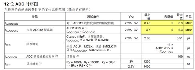
Part Number: MSP430F2419
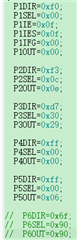
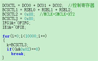
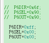
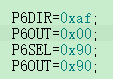
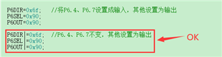
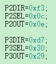
图所示为项目中MSP430F4219的初始化配置(XT2=8MHz),其中注释部分(P6)在调试时异常。
现象:
1、该段代码注释后系统正常运行;加入该段代码,系统无法完成管脚初始化配置;
2、将未注释的代码下载到另一个项目的板子(XT2=6MHz)上,管脚能正常初始化配置。
请教下大家,出现这种问题的原因以及解决的办法。谢谢!
Part Number: MSP430F2419
图所示为项目中MSP430F4219的初始化配置(XT2=8MHz),其中注释部分(P6)在调试时异常。
现象:
1、该段代码注释后系统正常运行;加入该段代码,系统无法完成管脚初始化配置;
2、将未注释的代码下载到另一个项目的板子(XT2=6MHz)上,管脚能正常初始化配置。
请教下大家,出现这种问题的原因以及解决的办法。谢谢!