Other Parts Discussed in Thread: MSP430F5526
请教TI工程师,
目前我在做的案子(24MH晶振,SMCLK和MCLK都选择24M频率),目前需要3MHz的频率;想通过配置USCI_B1配置成SPI master mode来产生一个3M的频率!
然后,现在打算参考ccs 中产生SPI的程序。
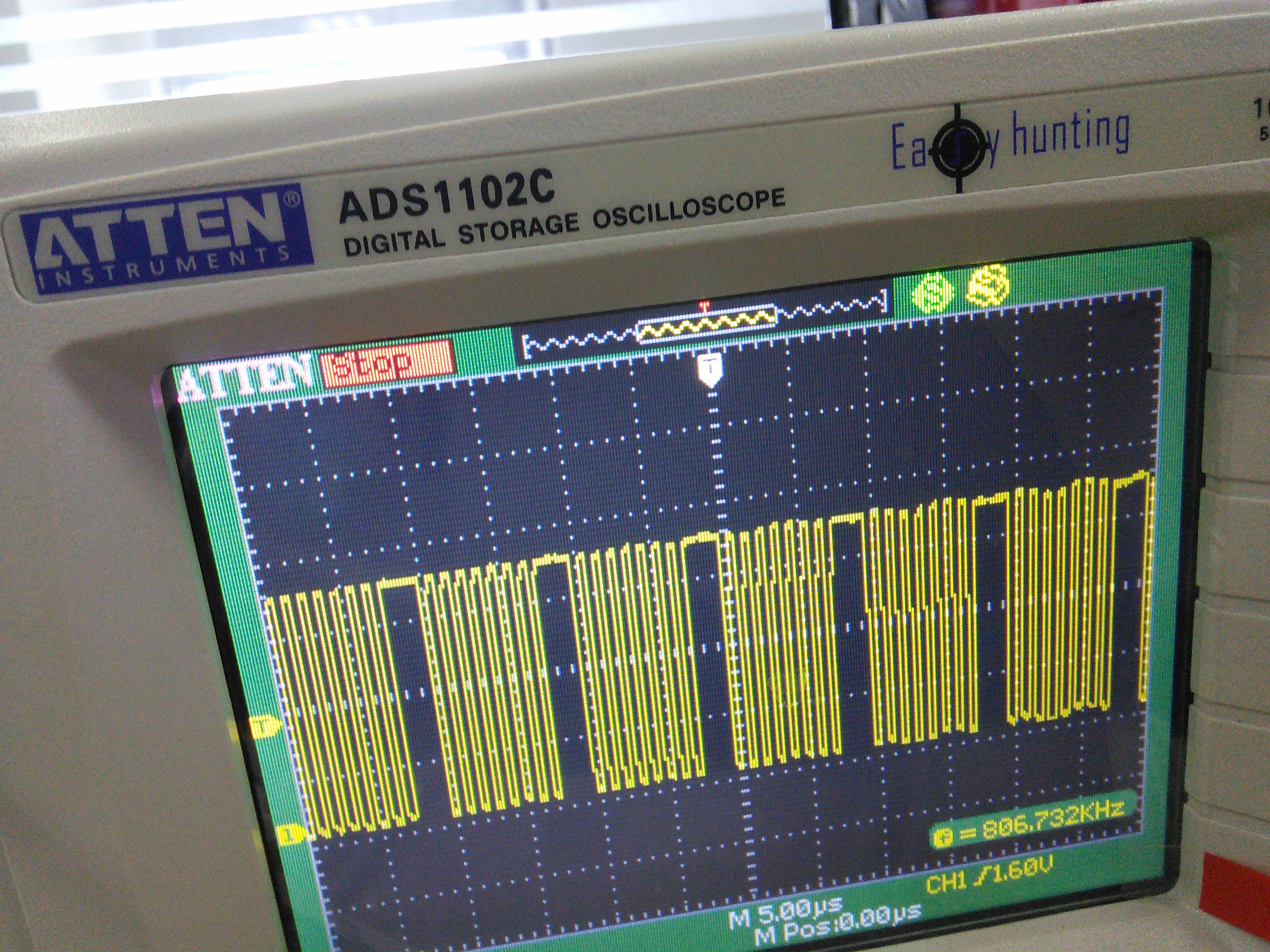
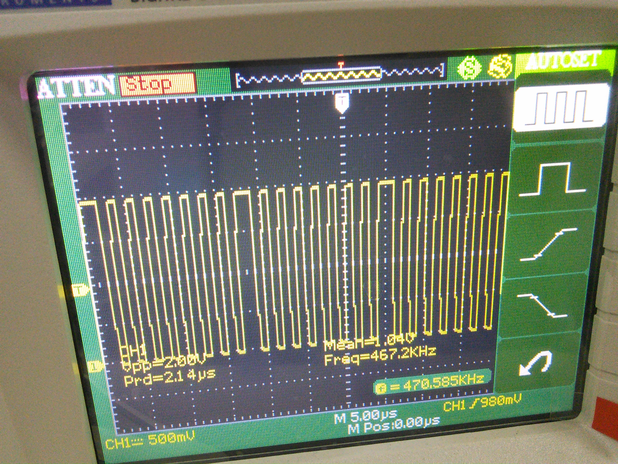
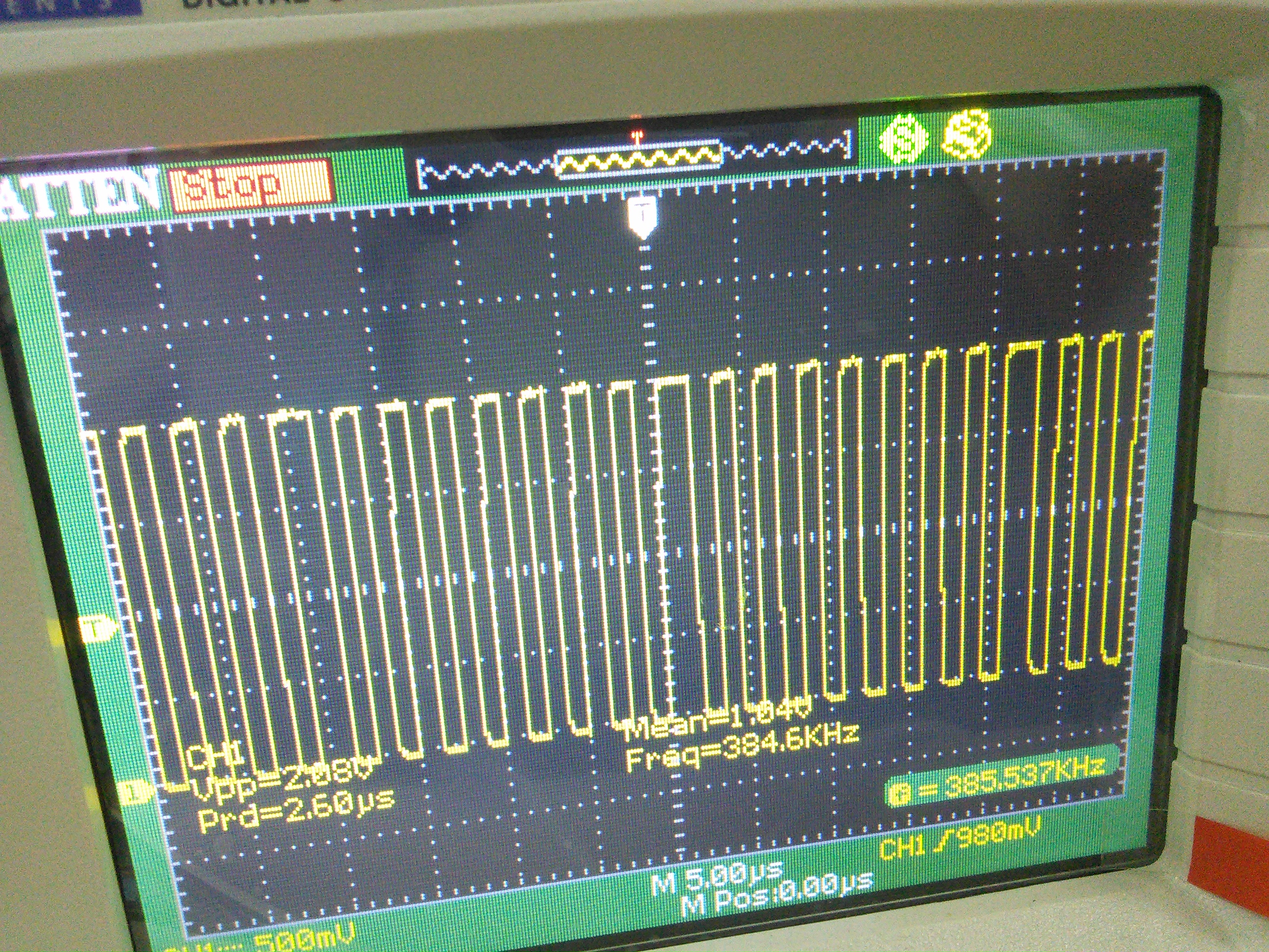
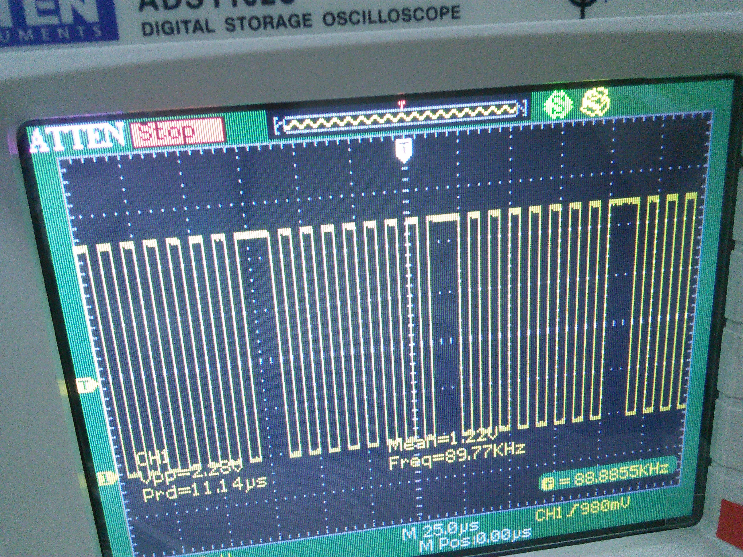
但是调试,CCS给的SPI例程发现,SPI产的波形并不是持续的时钟,而是断续的时钟:SPI是否可以产生持续的时钟
如下图所示:用示波器查看P4.3脚 CLK
// MSP430F552x
//                 -----------------
//             /|\|                 |
//              | |                 |
//              --|RST          P1.0|-> LED
//                |                 |
//                |             P3.4|-> Data Out (UCA0SIMO)
//                |                 |
//                |             P3.5|<- Data In (UCA0SOMI)
//                |                 |
//  Slave reset <-|P1.1         P3.0|-> Serial Clock Out (UCA0CLK)
//
//
//   Bhargavi Nisarga
//   Texas Instruments Inc.
//   April 2009
//   Built with CCSv4 and IAR Embedded Workbench Version: 4.21
//******************************************************************************

#include <msp430.h>

unsigned char MST_Data,SLV_Data;
unsigned char temp;

int main(void)
{
  volatile unsigned int i;

  WDTCTL = WDTPW+WDTHOLD;                   // Stop watchdog timer

  P1OUT |= 0x02;                            // Set P1.0 for LED
/*                                          // Set P1.1 for slave reset
  P1DIR |= 0x03;                            // Set P1.0-2 to output direction
  P3SEL |= BIT3+BIT4;                       // P3.3,4 option select
  P2SEL |= BIT7;                            // P2.7 option select

  UCA0CTL1 |= UCSWRST;                      // **Put state machine in reset**
  UCA0CTL0 |= UCMST+UCSYNC+UCCKPL+UCMSB;    // 3-pin, 8-bit SPI master
                                            // Clock polarity high, MSB
  UCA0CTL1 |= UCSSEL_2;                     // SMCLK
  UCA0BR0 = 0x02;                           // /2
  UCA0BR1 = 0;                              //
  UCA0MCTL = 0;                             // No modulation
  UCA0CTL1 &= ~UCSWRST;                     // **Initialize USCI state machine**
  UCA0IE |= UCRXIE;                         // Enable USCI_A0 RX interrupt

  P1OUT &= ~0x02;                           // Now with SPI signals initialized,
  P1OUT |= 0x02;                            // reset slave

  for(i=50;i>0;i--);                        // Wait for slave to initialize

  MST_Data = 0x01;                          // Initialize data values
  SLV_Data = 0x00;                          //

  while (!(UCA0IFG&UCTXIFG));               // USCI_A0 TX buffer ready?
  UCA0TXBUF = MST_Data;                     // Transmit first character

*/

/////
    P1DIR |= 0x03;                            // Set P1.0-2 to output direction
    P4SEL |= BIT1+BIT2+BIT3;                       // P3.3,4 option select
  //  P4DIR |= BIT3;                           // P2.7 option select

    UCB1CTL1 |= UCSWRST;                      // **Put state machine in reset**
    UCB1CTL0 |= UCMST+UCSYNC+UCCKPL+UCMSB;    // 3-pin, 8-bit SPI master
                                              // Clock polarity high, MSB
    UCB1CTL1 |= UCSSEL_2;                     // SMCLK
    UCB1BR0 = 0x02;                           // /2
    UCB1BR1 = 0;                              //
    //UCBxMCTL = 0;                             // No modulation
    UCB1CTL1 &= ~UCSWRST;                     // **Initialize USCI state machine**
    UCB1IE |= UCRXIE;                         // Enable USCI_A0 RX interrupt

    P1OUT &= ~0x02;                           // Now with SPI signals initialized,
    P1OUT |= 0x02;                            // reset slave

    for(i=50;i>0;i--);                        // Wait for slave to initialize

    MST_Data = 0x01;                          // Initialize data values
    SLV_Data = 0x00;                          //

    while (!(UCB1IFG&UCTXIFG));               // USCI_A0 TX buffer ready?
    UCB1TXBUF = MST_Data;                     // Transmit first character

///////////////////////////////////////////////////////////////////////////////////////
  __bis_SR_register(LPM0_bits + GIE);       // CPU off, enable interrupts

  while(1);
}

////////////////////////////////////////////////////////////////////
#pragma vector=USCI_B1_VECTOR
__interrupt void USCI_B1_ISR(void)
{
  volatile unsigned int i;

  switch(__even_in_range(UCB1IV,4))
  {
    case 0: break;                          // Vector 0 - no interrupt
    case 2:                                 // Vector 2 - RXIFG
      while (!(UCB1IFG&UCTXIFG));           // USCI_A0 TX buffer ready?

      if (UCB1RXBUF==SLV_Data)              // Test for correct character RX'd
        P1OUT |= 0x01;                      // If correct, light LED
      else
        P1OUT &= ~0x01;                     // If incorrect, clear LED

      MST_Data++;                           // Increment data
      SLV_Data++;
      UCB1TXBUF = MST_Data;                 // Send next value

      for(i = 20; i>0; i--);                // Add time between transmissions to
                                            // make sure slave can process information
      break;
    case 4: break;                          // Vector 4 - TXIFG
    default: break;
  }
}

////////////////////////////////////////////////////////////////////

/*
#pragma vector=USCI_A0_VECTOR
__interrupt void USCI_A0_ISR(void)
{
  volatile unsigned int i;

  switch(__even_in_range(UCA0IV,4))
  {
    case 0: break;                          // Vector 0 - no interrupt
    case 2:                                 // Vector 2 - RXIFG
      while (!(UCA0IFG&UCTXIFG));           // USCI_A0 TX buffer ready?

      if (UCA0RXBUF==SLV_Data)              // Test for correct character RX'd
        P1OUT |= 0x01;                      // If correct, light LED
      else
        P1OUT &= ~0x01;                     // If incorrect, clear LED

      MST_Data++;                           // Increment data
      SLV_Data++;
      UCA0TXBUF = MST_Data;                 // Send next value

      for(i = 20; i>0; i--);                // Add time between transmissions to
                                            // make sure slave can process information
      break;
    case 4: break;                          // Vector 4 - TXIFG
    default: break;
  }
}
*/
// -----------------
// /|\| |
// | | |
// --|RST P1.0|-> LED
// | |
// | P3.4|-> Data Out (UCA0SIMO)
// | |
// | P3.5|<- Data In (UCA0SOMI)
// | |
// Slave reset <-|P1.1 P3.0|-> Serial Clock Out (UCA0CLK)
//
//
// Bhargavi Nisarga
// Texas Instruments Inc.
// April 2009
// Built with CCSv4 and IAR Embedded Workbench Version: 4.21
//******************************************************************************
#include <msp430.h>
unsigned char MST_Data,SLV_Data;
unsigned char temp;
int main(void)
{
volatile unsigned int i;
WDTCTL = WDTPW+WDTHOLD; // Stop watchdog timer
P1OUT |= 0x02; // Set P1.0 for LED
/* // Set P1.1 for slave reset
P1DIR |= 0x03; // Set P1.0-2 to output direction
P3SEL |= BIT3+BIT4; // P3.3,4 option select
P2SEL |= BIT7; // P2.7 option select
UCA0CTL1 |= UCSWRST; // **Put state machine in reset**
UCA0CTL0 |= UCMST+UCSYNC+UCCKPL+UCMSB; // 3-pin, 8-bit SPI master
// Clock polarity high, MSB
UCA0CTL1 |= UCSSEL_2; // SMCLK
UCA0BR0 = 0x02; // /2
UCA0BR1 = 0; //
UCA0MCTL = 0; // No modulation
UCA0CTL1 &= ~UCSWRST; // **Initialize USCI state machine**
UCA0IE |= UCRXIE; // Enable USCI_A0 RX interrupt
P1OUT &= ~0x02; // Now with SPI signals initialized,
P1OUT |= 0x02; // reset slave
for(i=50;i>0;i--); // Wait for slave to initialize
MST_Data = 0x01; // Initialize data values
SLV_Data = 0x00; //
while (!(UCA0IFG&UCTXIFG)); // USCI_A0 TX buffer ready?
UCA0TXBUF = MST_Data; // Transmit first character
*/
/////
P1DIR |= 0x03; // Set P1.0-2 to output direction
P4SEL |= BIT1+BIT2+BIT3; // P3.3,4 option select
// P4DIR |= BIT3; // P2.7 option select
UCB1CTL1 |= UCSWRST; // **Put state machine in reset**
UCB1CTL0 |= UCMST+UCSYNC+UCCKPL+UCMSB; // 3-pin, 8-bit SPI master
// Clock polarity high, MSB
UCB1CTL1 |= UCSSEL_2; // SMCLK
UCB1BR0 = 0x02; // /2
UCB1BR1 = 0; //
//UCBxMCTL = 0; // No modulation
UCB1CTL1 &= ~UCSWRST; // **Initialize USCI state machine**
UCB1IE |= UCRXIE; // Enable USCI_A0 RX interrupt
P1OUT &= ~0x02; // Now with SPI signals initialized,
P1OUT |= 0x02; // reset slave
for(i=50;i>0;i--); // Wait for slave to initialize
MST_Data = 0x01; // Initialize data values
SLV_Data = 0x00; //
while (!(UCB1IFG&UCTXIFG)); // USCI_A0 TX buffer ready?
UCB1TXBUF = MST_Data; // Transmit first character
///////////////////////////////////////////////////////////////////////////////////////
__bis_SR_register(LPM0_bits + GIE); // CPU off, enable interrupts
while(1);
}
////////////////////////////////////////////////////////////////////
#pragma vector=USCI_B1_VECTOR
__interrupt void USCI_B1_ISR(void)
{
volatile unsigned int i;
switch(__even_in_range(UCB1IV,4))
{
case 0: break; // Vector 0 - no interrupt
case 2: // Vector 2 - RXIFG
while (!(UCB1IFG&UCTXIFG)); // USCI_A0 TX buffer ready?
if (UCB1RXBUF==SLV_Data) // Test for correct character RX'd
P1OUT |= 0x01; // If correct, light LED
else
P1OUT &= ~0x01; // If incorrect, clear LED
MST_Data++; // Increment data
SLV_Data++;
UCB1TXBUF = MST_Data; // Send next value
for(i = 20; i>0; i--); // Add time between transmissions to
// make sure slave can process information
break;
case 4: break; // Vector 4 - TXIFG
default: break;
}
}
////////////////////////////////////////////////////////////////////
/*
#pragma vector=USCI_A0_VECTOR
__interrupt void USCI_A0_ISR(void)
{
volatile unsigned int i;
switch(__even_in_range(UCA0IV,4))
{
case 0: break; // Vector 0 - no interrupt
case 2: // Vector 2 - RXIFG
while (!(UCA0IFG&UCTXIFG)); // USCI_A0 TX buffer ready?
if (UCA0RXBUF==SLV_Data) // Test for correct character RX'd
P1OUT |= 0x01; // If correct, light LED
else
P1OUT &= ~0x01; // If incorrect, clear LED
MST_Data++; // Increment data
SLV_Data++;
UCA0TXBUF = MST_Data; // Send next value
for(i = 20; i>0; i--); // Add time between transmissions to
// make sure slave can process information
break;
case 4: break; // Vector 4 - TXIFG
default: break;
}
}
*/