


請問各位,
目前採用此M4進行SPI的使用,在使用下採用示波器進行頻率及TX的量測,發現波形無法為"正方波"
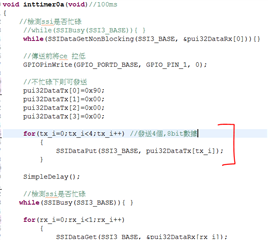
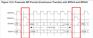
導致數據解析會異常,設置如下:
主頻:80Mhz
spi : 20Mhz
在自己設計得板子上與Tiva TM4C123G 开发板測試下波形都相同 (電路spi腳位部分皆無負載下量測)
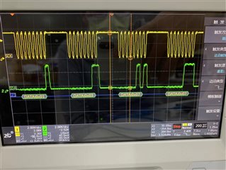
波形數據基本上與程式發送匹配,頻率量測也為20Mhz
只是頻率無法正方波
當此20Mhz逐漸下降,波形才會逐漸越正方
故.想請問大家,此ic是否有輸出頻率上限?? 或是是否需要搭配外部電路進行??
以上 謝謝

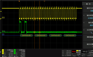
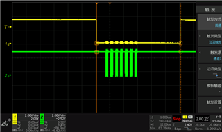
 上為FSS,下為LCK
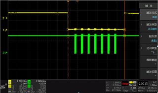 上為FSS,下為LCK
 上為FSS,下為LCK