This thread has been locked.

If you have a related question, please click the "Ask a related question" button in the top right corner. The newly created question will be automatically linked to this question.

TM4C123GH6PM 调试ADC时遇到的问题

Other Parts Discussed in Thread: TM4C123FH6PM, TM4C123GH6PM

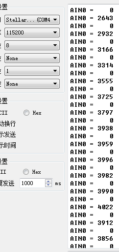
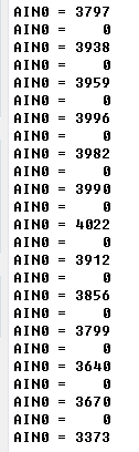
配置ADC0 四通道采样,软件触发,为什么每次采回的数据顺序都不一样,是跟溢出有关吗,请问怎样解决。测试代码如下:

#define ADC_Sequencer 1
#define ADC_BASE ADC0_BASE
void main(void) {

SysCtlClockSet(SYSCTL_SYSDIV_4|SYSCTL_USE_PLL|SYSCTL_XTAL_16MHZ|
SYSCTL_OSC_MAIN);

SystemClock=SysCtlClockGet();

MAP_SysCtlPeripheralEnable(SYSCTL_PERIPH_ADC0);
MAP_SysCtlPeripheralEnable(SYSCTL_PERIPH_GPIOD);
MAP_SysCtlPeripheralEnable(SYSCTL_PERIPH_GPIOE);

MAP_GPIOPinTypeADC(GPIO_PORTD_BASE, GPIO_PIN_1);
MAP_GPIOPinTypeADC(GPIO_PORTE_BASE, GPIO_PIN_2);
MAP_GPIOPinTypeADC(GPIO_PORTE_BASE, GPIO_PIN_1);
MAP_GPIOPinTypeADC(GPIO_PORTD_BASE, GPIO_PIN_2);


ADCSequenceConfigure(ADC_BASE, ADC_Sequencer, ADC_TRIGGER_PROCESSOR, 0);
ADCHardwareOversampleConfigure(ADC_BASE,8);
ADCSequenceStepConfigure(ADC_BASE, ADC_Sequencer, 0,
ADC_CTL_CH1);
ADCSequenceStepConfigure(ADC_BASE, ADC_Sequencer, 1,
ADC_CTL_CH2);
ADCSequenceStepConfigure(ADC_BASE, ADC_Sequencer, 2,
ADC_CTL_CH4);
ADCSequenceStepConfigure(ADC_BASE, ADC_Sequencer, 3,
ADC_CTL_IE | ADC_CTL_END | ADC_CTL_CH5);
ADCSequenceEnable(ADC_BASE, ADC_Sequencer);
ADCIntClear(ADC0_BASE, ADC_Sequencer);
ADCIntRegister(ADC0_BASE,ADC_Sequencer,ADC1IntHandler);
ADCIntEnable(ADC0_BASE,ADC_Sequencer);
IntMasterEnable();
while(1)
{
ADCProcessorTrigger(ADC_BASE, ADC_Sequencer);
SysCtlDelay(5000);
_nop();
}
}
void ADC1IntHandler()
{
ADCIntClear(ADC0_BASE, ADC_Sequencer);
ADCSequenceDataGet(ADC0_BASE, ADC_Sequencer, AD0IN4);
_nop();
}

  • 楼主可以参考官方多通道采样的例子。单通道采样时没有问题的么?

  • 请问哪有多通道的例程?

    我在采样的时候,一样的输入电压,经常采到差别很大的值,1.65V的电压直接接到PE3,采到的经常在1900和1200之间波动,不知道为什么?

    另外,我只接了PE3,为什么其他几路ADC也会采到很大的值,我用示波器测这些引脚,发现都有1-2V的电压,为什么呢

  • 参考tivaware中评估板对应的qs-logger历程。有用两个独立的ADC进行多通道采样的历程。

  • 我在采样的时候,一样的输入电压,经常采到差别很大的值,1.65V的电压直接接到PE3,采到的经常在1900和1200之间波动,不知道为什么?

    另外,我只接了PE3,为什么其他几路ADC也会采到很大的值,我用示波器测这些引脚,发现都有1-2V的电压,为什么呢

    不用的接地或接高,看是不是对的值,0或者FFF/FFE之类

  • 我试试去,不应该有这么大的误差的,除非你前级的电压本来误差就很大。而且你的这句话,用示波器量这些引脚,你用万用表量看看。

  • 好的,万用表倒是没测过,我试试

  • 不接高不接地,采样值不是000也不是fff,就是随机数

  • 这个是肯定的,因为这个电压是随机的,接VCC或者GND呢,AD的值是什么

  • TM4C123FH6PM的34、35、36不是xosc0和xosc1,可以使用实时时钟模块吗?文档说“在 RTC 模式中,要求 CCP0 输入时钟为 32.768 KHz。然后将时钟信号分频为 1 Hz,将其传送给计数器的输入端。”   CCP0是1脚或28脚,是不是把这些脚软件上配置成ccp0,硬件上接上晶振就可以呢

    TM4C123GH6PM是可以接一个32.768KHZ来使用实时时钟模块的。

  • 一脚应该是不可以的,因为手册上说,要使用32位实时时钟,定时器需要在CCP的偶数管脚上有一个32.768KHz的输入信号。是偶数管脚。

  • 再次看了看手册,TM4C123中有两个RTC,一个是定时器配置为RTC模式,一个需要用到CPP0引脚。一个是休眠模块的RTC,需要用到晶振或者内部振荡器,两者是不一样的。

  • 经过测试,悬空的时候,确实采集到的值会乱跳。AIN0接GND,在0-3之间跳动,接VCC,稳定采集4095,没你说的那么大的误差,也是用的LaunchPad

  • 我再试试,我测的是1.65V,跳的挺大。

  • //*****************************************************************************
    //
    // single_ended.c - Example demonstrating how to configure the ADC for
    //                  single ended operation.
    //
    // Copyright (c) 2010-2014 Texas Instruments Incorporated.  All rights reserved.
    // Software License Agreement
    // 
    //   Redistribution and use in source and binary forms, with or without
    //   modification, are permitted provided that the following conditions
    //   are met:
    //
    //   Redistributions of source code must retain the above copyright
    //   notice, this list of conditions and the following disclaimer.
    //
    //   Redistributions in binary form must reproduce the above copyright
    //   notice, this list of conditions and the following disclaimer in the
    //   documentation and/or other materials provided with the
    //   distribution.
    //
    //   Neither the name of Texas Instruments Incorporated nor the names of
    //   its contributors may be used to endorse or promote products derived
    //   from this software without specific prior written permission.
    // 
    // THIS SOFTWARE IS PROVIDED BY THE COPYRIGHT HOLDERS AND CONTRIBUTORS
    // "AS IS" AND ANY EXPRESS OR IMPLIED WARRANTIES, INCLUDING, BUT NOT
    // LIMITED TO, THE IMPLIED WARRANTIES OF MERCHANTABILITY AND FITNESS FOR
    // A PARTICULAR PURPOSE ARE DISCLAIMED. IN NO EVENT SHALL THE COPYRIGHT
    // OWNER OR CONTRIBUTORS BE LIABLE FOR ANY DIRECT, INDIRECT, INCIDENTAL,
    // SPECIAL, EXEMPLARY, OR CONSEQUENTIAL DAMAGES (INCLUDING, BUT NOT
    // LIMITED TO, PROCUREMENT OF SUBSTITUTE GOODS OR SERVICES; LOSS OF USE,
    // DATA, OR PROFITS; OR BUSINESS INTERRUPTION) HOWEVER CAUSED AND ON ANY
    // THEORY OF LIABILITY, WHETHER IN CONTRACT, STRICT LIABILITY, OR TORT
    // (INCLUDING NEGLIGENCE OR OTHERWISE) ARISING IN ANY WAY OUT OF THE USE
    // OF THIS SOFTWARE, EVEN IF ADVISED OF THE POSSIBILITY OF SUCH DAMAGE.
    // 
    // This is part of revision 2.1.0.12573 of the Tiva Firmware Development Package.
    //
    //*****************************************************************************
    
    #include <stdbool.h>
    #include <stdint.h>
    #include "inc/hw_memmap.h"
    #include "driverlib/adc.h"
    #include "driverlib/gpio.h"
    #include "driverlib/pin_map.h"
    #include "driverlib/sysctl.h"
    #include "driverlib/uart.h"
    #include "utils/uartstdio.h"
    
    //*****************************************************************************
    //
    //! \addtogroup adc_examples_list
    //! <h1>Single Ended ADC (single_ended)</h1>
    //!
    //! This example shows how to setup ADC0 as a single ended input and take a
    //! single sample on AIN0/PE7.
    //!
    //! This example uses the following peripherals and I/O signals.  You must
    //! review these and change as needed for your own board:
    //! - ADC0 peripheral
    //! - GPIO Port E peripheral (for AIN0 pin)
    //! - AIN0 - PE7
    //!
    //! The following UART signals are configured only for displaying console
    //! messages for this example.  These are not required for operation of the
    //! ADC.
    //! - UART0 peripheral
    //! - GPIO Port A peripheral (for UART0 pins)
    //! - UART0RX - PA0
    //! - UART0TX - PA1
    //!
    //! This example uses the following interrupt handlers.  To use this example
    //! in your own application you must add these interrupt handlers to your
    //! vector table.
    //! - None.
    //
    //*****************************************************************************
    
    //*****************************************************************************
    //
    // This function sets up UART0 to be used for a console to display information
    // as the example is running.
    //
    //*****************************************************************************
    void
    InitConsole(void)
    {
        //
        // Enable GPIO port A which is used for UART0 pins.
        // TODO: change this to whichever GPIO port you are using.
        //
        SysCtlPeripheralEnable(SYSCTL_PERIPH_GPIOA);
    
        //
        // Configure the pin muxing for UART0 functions on port A0 and A1.
        // This step is not necessary if your part does not support pin muxing.
        // TODO: change this to select the port/pin you are using.
        //
        GPIOPinConfigure(GPIO_PA0_U0RX);
        GPIOPinConfigure(GPIO_PA1_U0TX);
    
        //
        // Enable UART0 so that we can configure the clock.
        //
        SysCtlPeripheralEnable(SYSCTL_PERIPH_UART0);
    
        //
        // Use the internal 16MHz oscillator as the UART clock source.
        //
        UARTClockSourceSet(UART0_BASE, UART_CLOCK_PIOSC);
    
        //
        // Select the alternate (UART) function for these pins.
        // TODO: change this to select the port/pin you are using.
        //
        GPIOPinTypeUART(GPIO_PORTA_BASE, GPIO_PIN_0 | GPIO_PIN_1);
    
        //
        // Initialize the UART for console I/O.
        //
        UARTStdioConfig(0, 115200, 16000000);
    }
    
    //*****************************************************************************
    //
    // Configure ADC0 for a single-ended input and a single sample.  Once the
    // sample is ready, an interrupt flag will be set.  Using a polling method,
    // the data will be read then displayed on the console via UART0.
    //
    //*****************************************************************************
    int
    main(void)
    {
        //
        // This array is used for storing the data read from the ADC FIFO. It
        // must be as large as the FIFO for the sequencer in use.  This example
        // uses sequence 3 which has a FIFO depth of 1.  If another sequence
        // was used with a deeper FIFO, then the array size must be changed.
        //
        uint32_t pui32ADC0Value[1];
    
        //
        // Set the clocking to run at 20 MHz (200 MHz / 10) using the PLL.  When
        // using the ADC, you must either use the PLL or supply a 16 MHz clock
        // source.
        // TODO: The SYSCTL_XTAL_ value must be changed to match the value of the
        // crystal on your board.
        //
        SysCtlClockSet(SYSCTL_SYSDIV_10 | SYSCTL_USE_PLL | SYSCTL_OSC_MAIN |
                       SYSCTL_XTAL_16MHZ);
    
        //
        // Set up the serial console to use for displaying messages.  This is
        // just for this example program and is not needed for ADC operation.
        //
        InitConsole();
    
        //
        // Display the setup on the console.
        //
        UARTprintf("ADC ->\n");
        UARTprintf("  Type: Single Ended\n");
        UARTprintf("  Samples: One\n");
        UARTprintf("  Update Rate: 250ms\n");
        UARTprintf("  Input Pin: AIN0/PE7\n\n");
    
        //
        // The ADC0 peripheral must be enabled for use.
        //
        SysCtlPeripheralEnable(SYSCTL_PERIPH_ADC0);
    
        //
        // For this example ADC0 is used with AIN0 on port E7.
        // The actual port and pins used may be different on your part, consult
        // the data sheet for more information.  GPIO port E needs to be enabled
        // so these pins can be used.
        // TODO: change this to whichever GPIO port you are using.
        //
        SysCtlPeripheralEnable(SYSCTL_PERIPH_GPIOE);
    
        //
        // Select the analog ADC function for these pins.
        // Consult the data sheet to see which functions are allocated per pin.
        // TODO: change this to select the port/pin you are using.
        //
        GPIOPinTypeADC(GPIO_PORTE_BASE, GPIO_PIN_3);
    
        //
        // Enable sample sequence 3 with a processor signal trigger.  Sequence 3
        // will do a single sample when the processor sends a signal to start the
        // conversion.  Each ADC module has 4 programmable sequences, sequence 0
        // to sequence 3.  This example is arbitrarily using sequence 3.
        //
        ADCSequenceConfigure(ADC0_BASE, 3, ADC_TRIGGER_PROCESSOR, 0);
    
        //
        // Configure step 0 on sequence 3.  Sample channel 0 (ADC_CTL_CH0) in
        // single-ended mode (default) and configure the interrupt flag
        // (ADC_CTL_IE) to be set when the sample is done.  Tell the ADC logic
        // that this is the last conversion on sequence 3 (ADC_CTL_END).  Sequence
        // 3 has only one programmable step.  Sequence 1 and 2 have 4 steps, and
        // sequence 0 has 8 programmable steps.  Since we are only doing a single
        // conversion using sequence 3 we will only configure step 0.  For more
        // information on the ADC sequences and steps, reference the datasheet.
        //
        ADCSequenceStepConfigure(ADC0_BASE, 3, 0, ADC_CTL_CH0 | ADC_CTL_IE |
                                 ADC_CTL_END);
    
        //
        // Since sample sequence 3 is now configured, it must be enabled.
        //
        ADCSequenceEnable(ADC0_BASE, 3);
    
        //
        // Clear the interrupt status flag.  This is done to make sure the
        // interrupt flag is cleared before we sample.
        //
        ADCIntClear(ADC0_BASE, 3);
    
        //
        // Sample AIN0 forever.  Display the value on the console.
        //
        while(1)
        {
            //
            // Trigger the ADC conversion.
            //
            ADCProcessorTrigger(ADC0_BASE, 3);
    
            //
            // Wait for conversion to be completed.
            //
            while(!ADCIntStatus(ADC0_BASE, 3, false))
            {
            }
    
            //
            // Clear the ADC interrupt flag.
            //
            ADCIntClear(ADC0_BASE, 3);
    
            //
            // Read ADC Value.
            //
            ADCSequenceDataGet(ADC0_BASE, 3, pui32ADC0Value);
    
            //
            // Display the AIN0 (PE7) digital value on the console.
            //
            UARTprintf("AIN0 = %4d\r\n", pui32ADC0Value[0]);
    
            //
            // This function provides a means of generating a constant length
            // delay.  The function delay (in cycles) = 3 * parameter.  Delay
            // 250ms arbitrarily.
            //
            SysCtlDelay(SysCtlClockGet() / 12);
        }
    }
    

    这是我测试的例程,用的是PE3,AIN0

  • 由于串口问题,我只能用的单步调试看的变量的值,我是用杜邦线连接PE3和函数信号发生器,刚刚试了这段代码,循环多次,采样值也是跳动很大,难道是我的测试电路不对吗?  

    不知道您是怎么输入电压信号到PE3的?您是通过串口来看采样值的吧

  • 我是通过串口打印输出值的,杜邦线直接连接PE3和VCC和GND打印输出的。你是如何测试的呢?串口不能用的话,CCS单步调试,看这个值的变化吧。

  • 循环多次,值变化蛮大的,来去1000都有

  •   你看,这是我搞定串口后用你给的程序测的。来去已经变小了,但是还是有一两百多

  • 首先怀疑你外部输入的信号波动就是这么大的问题。你接VCC试试,肯定不会这么跳的厉害的。

  • 为什么我的示波器纵轴显示范围一直在86到326??前半部分的曲线看不到,不管观测值如何变化,超过326和低于86的值就看不到。

    重新建立示波器,范围会变化,但是曲线还是会上下的削顶超出范围,而不能全部显示。

    按了那个放大镜,应该是自适应,选择了both方向,也没什么用

  • 什么叫做悬空呀,测试的时候不是直接接到PE3吗

  • 我用杜邦线直接连接PE3和GND,输出值是3或4或5,连接VCC是4095,但是直接外接一个电压用万用表测了,电压稳定,输出值是0、4095,中间还加一些其他的数,完全不是我要测的电压,电压在0-3.3的,还是外接的时候要接上其他接口,

  • 您好,我在测4路的时候也遇到这些问题测出的数据不准,调动很大,您是怎么解决的

  • 您是将杜邦线怎么直接将PE3、VCC以及GND连接起来,在接收的时候不能直接连接吗,如果有多路信号那该如何去做