This thread has been locked.

If you have a related question, please click the "Ask a related question" button in the top right corner. The newly created question will be automatically linked to this question.

UCC21550: 驱动输出电阻的理解

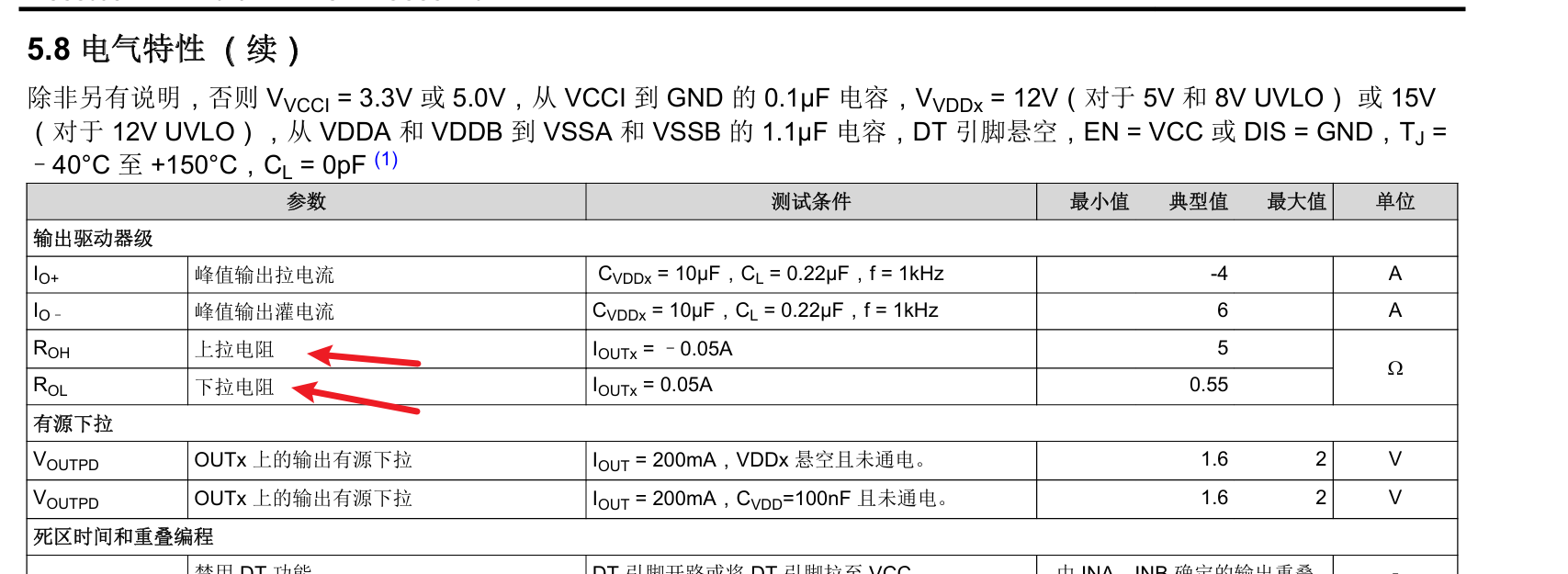
Part Number: UCC21550

image.png这个输出电阻怎么理解,是不是可以理解为等效的驱动回路的电阻是:驱动芯片的输出电阻+串联的门级电阻+mos内部的Rg,因此如果驱动电压为20V,外部不串联电阻,mos内部Rg为9欧姆,驱动芯片的输出电阻为1欧,那最大的输出电流就只有2A,是这么理解吗?恳请解答

  • 您好

    The UCC21550 output stages feature a pull-up structure which delivers the highest peak-source current when it is most needed, during the Miller plateau region of the power-switch turn on transition (when the power switch drain or collector voltage experiences dV/dt). The output stage pull-up structure features a P-channel MOSFET and an additional Pull-Up N-channel MOSFET in parallel. The function of the N-channel MOSFET is to provide a brief boost in the peak-sourcing current, enabling fast turn on. This is accomplished by briefly turning on the N-channel MOSFET during a narrow instant when the output is changing states from low to high. The ROH parameter is a DC measurement and it is representative of the on-resistance of the P-channel device only. This is because the Pull-Up N-channel device is held in the off state in DC condition and is turned on only for a brief instant when the output is changing states from low to high. This N-channel device has an on-resistance of approximately 1.47 Ω. Therefore, the effective resistance of the UCC21550 pull-up stage during this brief turn-on phase is the parallel resistance between the pull-up NMOS and pull-up PMOS, which is 1.47Ω // 5Ω, much lower than what is represented by the ROH parameter. The value of ROH belies the fast nature of the UCC21550 turn-on time. The pull-down structure in the UCC21550 is simply composed of an N-channel MOSFET. The ROL parameter, which is also a DC measurement, is representative of the impedance of the pull-down state in the device. Both outputs of the UCC21550 are capable of delivering 4-A peak source and 6-A peak sink current pulses. The output voltage swings between VDD and VSS provides rail-to-rail operation, thanks to the MOS-out stage which delivers very low drop-out.

    这是datasheet给出相关详细说明,请您参考

  • thank you very much