This thread has been locked.
If you have a related question, please click the "Ask a related question" button in the top right corner. The newly created question will be automatically linked to this question.
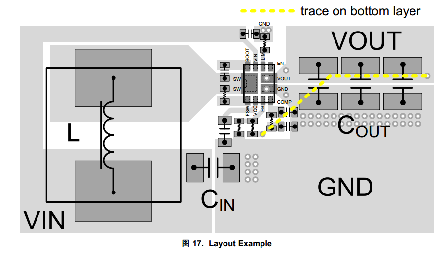
手册中的示例如上图,
其中“大面积”的布线是怎么实现的?放置的铜皮(Place--Fill)?
Hi
利用PCB上的敷铜,这个是PCB板上有的,PCB厂商会做的。
如果你使用Altium Designer设计软件,就选place polygon plane,然后选择你要覆铜的电气属性(如GND, Vin等),再勾勒出铜的面积形状就可以了