

您好:
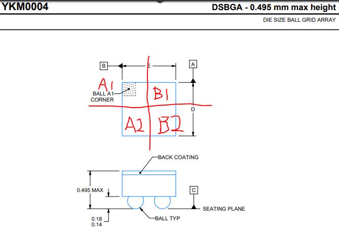
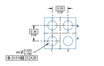
需要帮忙确认下芯片封装问题,如下是YKM的封装图,按照前面的说明,从正面看左上角应该是A1脚,正常理解左下角是A2脚,右上角是B1脚,右下角是B2脚,不知道是否正确?
但是按照后面的图片看左下角是A1脚,右下角是A2脚,和前图不一致。
请帮忙确认下如何确认脚位?谢谢。
您好:
需要帮忙确认下芯片封装问题,如下是YKM的封装图,按照前面的说明,从正面看左上角应该是A1脚,正常理解左下角是A2脚,右上角是B1脚,右下角是B2脚,不知道是否正确?
但是按照后面的图片看左下角是A1脚,右下角是A2脚,和前图不一致。
请帮忙确认下如何确认脚位?谢谢。