This thread has been locked.

If you have a related question, please click the "Ask a related question" button in the top right corner. The newly created question will be automatically linked to this question.

BQ76930: 充电问题

Part Number: BQ76930
Other Parts Discussed in Thread: TIDA-01093

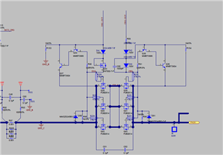
两片BQ76930级联监测20S电池。充电MOS和放电MOS管的关断和开启通过MCU分别读取两个BQ76930的CHG和DSG的状态后,MUC控制逻辑芯片(输出12V)来控制MOS管的开和关。在测试充电时发现在关断充电MOS、开启放电MOS时,连接充电器发现可以充电;并且充电MOS发热严重,此时Vgs=3.65V、Vds=3.6V;断开充电器后Vgs、Vds就没有电压了。这是什么原因导致的?

  • 您好,由于问题比较复杂,我需要询问更了解这款芯片的TI工程师,再帮您解答,稍后回复

  • 您好,请参考虾面的内容:

    It looks like the design followed the basic structure of TIDA-01093 for a FET circuit.  The issue seems to be that they should have kept the Q31 of TIDA-01093 so that the charge gate voltage can fall with PACK- when a charger is applied.  As is, with the charger applied at a voltage greater than the battery and CHG_OUT low, the signal from the 12V logic chip which drives CHG_OUT can't go significantly below GND_B, perhaps -0.2V.  D42 and D44 will both be forward biased at perhaps 0.5V each putting the gate of the FET at about -0.6 to -1 V.  VGSTH of the FET is between 3 and 5 V, from the measurement about 3.65 V, so the FET will act as a source follower and the difference between the battery and charger will drop across the body diode of (Q42) and the charge FET (Q43) VGS.

    Include the P-ch such as Q3 in figure 8 of the BQ76930 data sheet or Q31 of TIDA-01093 after the 12V logic chip output.  This will allow the Q42 gate voltage to fall and Q42 etc to stay off when the 12V logic chip output is low.